GeistHaus
log in · sign up

Silicon Junction

Part of wordpress.com

stories
Stop Hating SMPS: Clean Audio Power from Laptop Bricks
AudioPoweraudio electronicsaudiophile DIYcapacitance multiplierinductor selectionlaptop brickLC filterMLCC capacitorsPCB layoutpower supply filteringpower supply noiseSMPSswitching noiseSziklai pair
The audiophile world has long treated switched-mode power supplies as the enemy — noisy, compromised, something to be tolerated in budget gear but never trusted where sound quality matters. Browse almost any forum thread about powering a DAC or headphone amp and you’ll find the same orthodoxy: linear regulators only, toroidal transformers preferred, massive filter […]
Show full content

The audiophile world has long treated switched-mode power supplies as the enemy — noisy, compromised, something to be tolerated in budget gear but never trusted where sound quality matters. Browse almost any forum thread about powering a DAC or headphone amp and you’ll find the same orthodoxy: linear regulators only, toroidal transformers preferred, massive filter banks mandatory, and cheap SMPS strictly forbidden.

But this reputation isn’t entirely warranted. With carefully chosen filtering components, a basic understanding of where noise actually lives, and some layout discipline, a quality laptop brick can deliver surprisingly clean rails to an audio circuit. The noise produced by SMPS is largely predictable and filterable.

This article is about repurposing the laptop brick as an audiophile-quality supply. We’ll look at where SMPS noise comes from, why it’s more manageable than its reputation suggests, and what simple measures let you extract genuinely clean power from a supply that most audiophiles would throw in a drawer.

If you are impatient, feel free to jump straight to the results.

What You’ll Need

The Best Consumables (AliExpress | Amazon)

0805 SMT Resistors Kit (AliExpress | Amazon)

TIP32C PNP Power Transistors (AliExpress | Amazon)

SMT Aluminium Polymer Capacitor Kit (AliExpress | Amazon)

0805 SMT MLCC Capacitors Kit (AliExpress | Amazon)

5.5×2.1mm PCB Mount DC Socket (AliExpress | Amazon)

The EasyEDA project (schematic + pcb) if you want to order your own PCB (BSD License)

Understand the enemy

The first thing we’re going to do is have a close look at the noise of several laptop PSUs. I selected three from my junk drawer and applied a 1 kΩ load to simulate audio gear at idle. Light loads are typically the worst-case for switching noise.

I then captured the output from all three bricks:

Brick 1
Brick 2
Brick 3

The noise profiles of all three are relatively similar, and share a common feature: repetitive bursts of high-frequency oscillations, typically centered around 20 MHz.

We’ll now focus on Brick 3, which had by far the highest switching noise of the three with noise at ~600 mVpp — a useful worst-case to design against. Taking a more detailed capture:

Detailed capture of Brick 3’s noise bursts.

From the detailed capture, the bursts repeat at 4.7 kHz — right in the audio band. This is lower than you might expect from an SMPS, but at light loads most modern controllers deliberately switch into burst mode to maintain efficiency, trading a higher switching frequency for short, periodic packets of switching activity.

We’ll now zoom in all the way and take a capture of a single burst:

Capture of a single noise burst.

The burst lasts just 1 µs and contains oscillations ranging from roughly 2 MHz to 20 MHz — a broad spread of high-frequency energy.

Let’s take an FFT of a single burst:

FFT of a single laptop brick noise burst

The majority of the noise is centered around 17 MHz, spreading roughly 5 MHz either side and falling off quickly above 22 MHz.

Less is Sometimes More

This high-frequency noise is exactly why SMPS supplies get such a bad reputation among audio builders — and why many well-intentioned filtering attempts fall short.

When I first started experimenting with these supplies, my instinct was the same as everyone else’s: bigger inductance, bigger capacitance, more filtering.

The problem is that an inductor doesn’t just provide inductance — it also has a parallel capacitance, formed between individual windings. The more windings, the greater the inter-winding capacitance, and the lower the frequency at which that capacitance takes over. Above this self-resonant frequency, the inductor stops behaving like an inductor entirely and starts looking like a capacitor. At 17 MHz, a poorly chosen inductor isn’t filtering anything — it’s just a capacitor in series with your supply rail, allowing high-frequency noise to pass straight through unimpeded.

The same is true of capacitors: larger values generally imply more internal structure, increasing parasitic inductance, and beyond a certain point they can no longer effectively shunt noise to ground.

Closing In On A Solution

Now that we have a clearer understanding of the challenges, we can begin to develop an effective solution. One key insight is that it won’t be possible to eliminate all noise using a single filtering stage. Instead, a two-stage filter design is required.

The first stage will target the highest-frequency noise, while a second stage will handle lower-frequency components.

This approach targets differential-mode noise present on the supply rails. Switching supplies can also generate common-mode noise through parasitic coupling across the isolation barrier — a separate problem not addressed by a simple LC filter.

In applications where this becomes an issue, a common-mode choke placed at the output of the SMPS can be used to attenuate it before it enters the rest of the system. In my testing across several grounded systems, however, I didn’t encounter any practical issues attributable to common-mode noise, so no additional filtering was required.

First Stage

For the first stage, we’ll use a low-pass LC filter topology, with careful component selection being critical to overall performance.

Inductor Selection

The inductor must maintain good performance well beyond 22 MHz while handling the required load current without saturating. More inductance isn’t always better here — as we established earlier, a larger inductor brings more inter-winding capacitance and a lower self-resonant frequency (SRF), which can undermine filter performance entirely at high frequencies.

A promising option is the TDK SPM6530T series of shielded power inductors, offering inductance values from 0.25 µH to 10 µH with saturation currents ranging from 28.5 A down to 3.8 A.

TDK SPM6530T series+
L (µH)ToleranceL Measuring Frequency (kHz)DC Resistance (mΩ) maxDC Resistance (mΩ) typIsat (A) typItemp (A) typPart No.0.25±20%1002.312.1028.523.0SPM6530T-R25M2300.47±20%1003.633.3020.520.0SPM6530T-R47M1700.56±20%1003.633.3020.520.0SPM6530T-R56M0.68±20%1005.394.9016.616.0SPM6530T-R68M1401.0±20%1007.817.1014.113.0SPM6530T-1R0M1201.5±20%10010.79.7011.511.0SPM6530T-1R5M1002.2±20%10019.117.38.48.2SPM6530T-2R2M3.3±20%10029.727.07.36.8SPM6530T-3R3M4.7±20%10039.435.86.25.6SPM6530T-4R7M6.8±20%10053.348.44.04.0SPM6530T-6R8M10±20%10072.565.93.83.6SPM6530T-100M

The higher inductance values in this series have saturation currents approaching the ~5 A output of a typical laptop supply, leaving insufficient margin, so we can immediately narrow the field to the 0.25 µH to 2.2 µH variants.

Next, we evaluate the high-frequency performance:

SPM6530 Frequency Characteristics

The frequency characteristics chart allows us to narrow the field further. The 2.2 µH inductor’s inductance begins rising in the 20–30 MHz range — a sign that it is approaching its SRF (Self Resonant Frequency) — which rules it out.

The 0.47 µH inductor, by contrast, remains stable to around 40 MHz with an SRF of approximately 90 MHz, giving us comfortable margin above our 22 MHz target. There is no strong justification for going smaller than this, which rules out the 0.25 µH option.

This leaves us with the 0.47 µH, 0.56 µH, 1.0 µH, and 1.5 µH inductors, all of which are likely to meet our requirements. Lower inductance values tend to favor higher current handling and better high-frequency performance, while higher values may provide improved noise attenuation at lower frequencies.

Corner frequency calculations showed that 0.47 µH was already sufficient for our target filter response, and a lower inductance value means lower DC resistance and less voltage drop under load — so the 0.56 µH and 1.5 µH were set aside. At just 14 cents each, I ordered both the 0.47 µH and 1.0 µH for evaluation.

Capacitor Selection

The capacitor selection is guided by three requirements: low impedance at 22 MHz, sufficient capacitance after DC bias derating, and a package size appropriate for high-frequency use.

For package size, 0805 is a reasonable choice at these frequencies — smaller packages have lower parasitic inductance, but 0805 strikes a good balance between high-frequency performance and ease of hand soldering.

Murata’s SimSurfing tool is invaluable here, providing DC bias derating curves and impedance plots for every part in their catalogue. The selected part is the Murata GRM21BR61H106KE43L — a 10 µF, 50 V, X5R capacitor in 0805.

SimSurfing reveals two important characteristics of this capacitor. First, the DC bias derating is significant — at 19 V the nominal 10 µF drops to just 1.7 µF. This is a property of multi-layer ceramic capacitors (MLCC) that often catches builders off guard: unlike film or electrolytic types, MLCCs lose capacitance as the DC bias voltage increases.

DC Bias vs Capacitance

Second, the self-resonant frequency is at 2 MHz, where |Z| reaches a minimum of 0.004 Ω. By 22 MHz the capacitor is behaving inductively and |Z| has risen to 0.05 Ω.

Frequency vs |Z|

That last figure might look alarming, but context matters. At 22 MHz the inductor presents around 50–60 Ω of impedance, making the capacitor’s 0.05 Ω utterly negligible by comparison. The filter is still working effectively even though the capacitors are operating above their SRF.

To address the DC bias derating, six capacitors are placed in parallel. This recovers the nominal capacitance — 6 × 1.7 µF = 10.2 µF at operating voltage — which keeps the math simple and, as a bonus, paralleling capacitors reduces the effective ESL and pushes the combined SRF higher. The PCB layout leaves pads for all six in parallel, with room to experiment with overlapping or decade values if desired.

Corner Frequency

With component values finalised — 0.47 µH and 10 µF effective capacitance after DC bias derating — we can verify the corner frequency:

f−3dB=12πLC=12π470×10−9×10×10−6≈73 kHz\begin{align} f_{-3\text{dB}} &= \frac{1}{2\pi\sqrt{LC}} \\ &= \frac{1}{2\pi\sqrt{470 \times 10^{-9} \times 10 \times 10^{-6}}} \approx 73\text{ kHz} \end{align}

What we actually care about is the attenuation at 17 MHz, where the bulk of the switching noise’s energy resides. A second-order LC filter rolls off at 40 dB per decade:

decades=log10⁡(fnoisef−3dB)=log10⁡(17 MHz73 kHz)≈2.37\begin{align} \text{decades} &= \log_{10}\left(\frac{f_{\text{noise}}}{f_{-3\text{dB}}}\right) \\ &= \log_{10}\left(\frac{17\text{ MHz}}{73\text{ kHz}}\right) \approx 2.37 \end{align}

With 17 MHz sitting 2.37 decades above the corner frequency, the attenuation is:

2.37 × 40 dB ≈ 95 dB.

That is a substantial amount of rejection. The residual low-frequency envelope of the switching bursts is left to the second stage to handle.
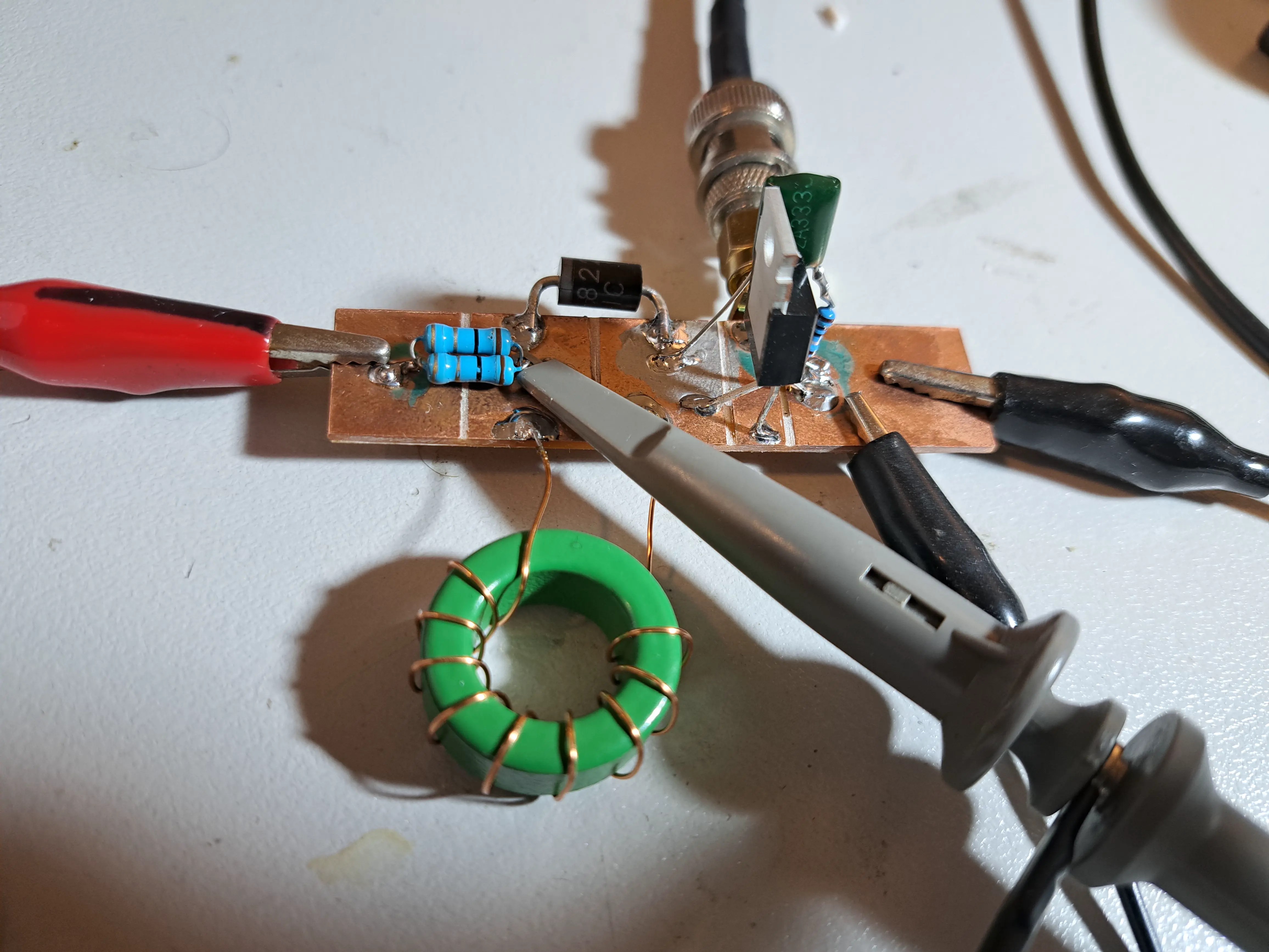
Schematic
First Stage: High Frequency LC Filter

L1 and C1–C6 form the low-pass filter. Layout matters here — the capacitors must sit as close as possible to L1 and have a solid ground connection, achieved with generous via stitching.

The six capacitor pads allow experimentation to validate which combination of values gives the best filtering performance.

Second Stage: Active Filter

The second stage can be implemented in several ways — a conventional linear regulator is the natural choice for most builds. In my design, I used a capacitance multiplier instead, for a few reasons specific to this application:

  • The filter bandwidth is adjustable.
  • The circuit acts as a filter rather than regulating to a fixed output.
  • Multiple output stages can be paralleled easily for higher current capacity.

However, by using a capacitance multiplier I’ve introduced a potentially bigger issue — this circuit has no thermal or over-current protection. A short circuit or sustained overload will push the Sziklai pairs into a condition where they are dissipating significant power with no way to limit it. In a linear regulator this is handled internally; here, it falls entirely to the system designer.

If your load is well-characterized and benign, this may not concern you. If there is any risk of a short or fault condition, a fuse on the input is the minimum precaution — a fast-blow type rated just above your maximum expected load current.

Thermal management deserves similar attention. The Sziklai pairs will dissipate power equal to the voltage drop across them multiplied by the load current. At higher currents this can become substantial, and the transistors must be mounted to adequate heatsinks. Paralleling additional output stages distributes this dissipation, which is one of the practical advantages of the topology.

R2 and C11 form an RC filter providing a stable reference voltage that feeds one or more Sziklai pair emitter followers. The cutoff frequency of the RC network is:

f−3dB=12πRC=12π×330×330×10−6≈1.46 Hz\begin{align} f_{-3\text{dB}} &= \frac{1}{2\pi RC} \\ &= \frac{1}{2\pi \times 330 \times 330 \times 10^{-6}} \approx 1.46\text{ Hz} \end{align}

1.46 Hz — an extraordinarily low corner frequency — essentially DC.

Each Sziklai pair includes a small ballast resistor (R1) to improve load sharing between multiple pairs, and a base resistor (R3) connected to VCC to improve turn-off time by providing a path for current to flow into Q2‘s base.

The Sziklai configuration is chosen over a single power transistor for two reasons. First, the increased composite beta means significantly less current is drawn from the RC reference network, preserving the stability of the reference voltage that the filter’s performance depends on. Second, Sziklai pairs have only a single (~0.7 V) base-emitter drop, while a Darlington has two (~1.4 V total). This reduces the voltage drop across the output stage, which reduces dissipation and leaves more of our initial voltage available at the output.

Results

I ordered a PCB from JLCPCB and populated it with the component values calculated earlier. A single heatsink spans all three output stages, thermally coupling them together to improve load balancing.

The filter as built can handle up to 5–6 A (approximately 100 W at 19 V), with a voltage drop of just 0.9–1.1 V across the full load range — remarkably flat. At full load this corresponds to around 6–8 W of dissipation, or approximately 95% efficiency.

The finished filter. Contains only ~$5 of components total. Considerably cheaper than building a linear supply.
100 W dummy load: two 8 Ω resistors in parallel, clamped to an aluminum heat-sink with thermal paste. Approximate engineering at its finest.

With the board assembled, it’s time to see how the filter performs in practice.

First, we take a capture before and after the first stage filter:

Raw noise present on the input
Noise present after the first filter stage

Before the first stage LC filter we observe a ripple of 584 mVpp, and after only 37 mVpp. An amplitude reduction of ~15×, an excellent initial result.

However, this amplitude isn’t the whole story. The real question is whether the high-frequency switching noise has been attenuated. Zooming in:

Zoomed view of noise present after the first filter stage

The high-frequency noise is gone. What remains are a few decaying oscillations at approximately 50 kHz — exactly the frequency range the second stage is designed to handle.

Finally, let’s examine the output of the final filter stage:

Output of the final filter stage

The output ripple is less than 1.6 mVpp, a reduction of over 300× from the raw 584 mVpp we started with.

The 1.6 mVpp shown here is the limit of what I’m able to reliably measure with this setup — with the probe shorted to its own ground I still read 1.6 mVpp, meaning the true output noise lies below this measurement floor. This noisy laptop brick has been repurposed for audiophile duty.

As they say, the proof of the pudding is in the eating. So as a final test I built a small one-transistor Class A amplifier and recorded the output when it was running on the laptop brick with and without the filter. You can listen to the results:

Amplifier output running on laptop SMPS with no filter
Amplifier output running on filtered laptop SMPS

Download audio
Download audio
https://siliconjunction.top/?p=3756
Extensions
Every Diode is a Varactor in Disguise
Bench Tests1SV149AM tuningBJTdepletion regiondiodeelectronicsjunction capacitanceLEDMOSFET body diodeRFSchottkysemiconductorsilicon rectifiertest harnesstunable filtervaractorvoltage controlled oscillator
A capacitor, at its core, is just two conducting plates separated by an insulating layer. Charge accumulates on the plates, an electric field spans the gap, and energy is stored. It’s one of the most fundamental structures in electronics — and it turns out that structure exists naturally inside every diode. When a diode is […]
Show full content

A capacitor, at its core, is just two conducting plates separated by an insulating layer. Charge accumulates on the plates, an electric field spans the gap, and energy is stored. It’s one of the most fundamental structures in electronics — and it turns out that structure exists naturally inside every diode.

When a diode is reverse biased, a region forms at the p-n junction called the depletion region. Free charge carriers — electrons on the n-side, holes on the p-side — are pushed away from the junction, leaving behind a zone that is swept clean of mobile charges. This makes it a poor conductor, much like the dielectric in a capacitor. On either side, the bulk doped semiconductor remains conductive, acting like the plates. Two conductive regions, separated by an insulating layer: it’s a capacitor, built right into the junction.

Increasing the reverse bias voltage increases the width of the depletion region

What makes this interesting is that the depletion region doesn’t have a fixed width. Increase the reverse voltage, and it widens — effectively pulling the plates further apart and reducing the capacitance. Decrease the voltage, and it narrows, increasing the capacitance. The relationship follows a curve determined by the doping profile of the junction, but the core idea is simple: you have a capacitance that you can control just by adjusting a DC voltage.

The Varactor

A component whose capacitance you can tune with a voltage is a useful thing — useful enough that a whole class of diode was developed around the idea. They’re called varactors, short for variable reactor, and they’re a staple of RF circuits, voltage-controlled oscillators, and tunable filters. But dedicated varactors are simply diodes optimized and characterized for this effect — every p-n junction diode already has it.

Every Other Diode

So if every p-n junction is hiding a varactor, the natural question is: how usable are they in practice? Dedicated varactors are characterized with precise capacitance-voltage curves and tight tolerances — but a bag of 1N4148s or a strip of LEDs pulled from a drawer? Not so much. To find out, I put a handful of common, everyday components into a test harness and measured how their junction capacitance varies with reverse voltage. The results might change what you reach for next time you need a tunable capacitor.

What You’ll Need

Polyester Film Capacitors Kit (AliExpress | Amazon)

Resistors Kit (AliExpress | Amazon)

1SV149 Varactor Diode (AliExpress | Amazon)

Test Harness

The test harness mirrors the topology a varactor would typically see in a real circuit. C1 is a DC blocking capacitor, isolating the bias voltage from the rest of the circuit. Because C1 appears in series with the varactor D1, it needs to be significantly larger in value — otherwise it will dominate the series combination and compress the effective tuning range.

The bias voltage is applied to the varactor through R1, which must be a high value to prevent it from loading the junction and disturbing the capacitance measurement.

The test harness used to qualify devices

To get a representative picture of what’s out there in a typical parts bin, I tested a range of common components: standard silicon rectifier diodes, fast signal diodes, Schottky diodes, LEDs, and BJT transistors — using the base-collector junction. I also threw in a selection of MOSFETs, using the body diode that exists inherently in every device.

To use an N-channel MOSFET’s body diode as a varactor, connect the gate and source together and treat this as the anode. The drain serves as the cathode.

A P-channel do the same thing, but the drain is the anode and the source is the cathode..

Here is a table of the results:

Device@ 1V (pF)@ Vmax (pF)Vmax (V)Tuning Ratio1SV149440.922.17919.89IRFP46058424483013.04NCE65T540F2912238.63012.20IRF540N1759.8225.2327.811N5822290.364.84304.48IRLZ44N974221.8304.391N581964.2214.65304.381N540437.413.62302.752N700013.765.57322.471N5711114.58322.40TIP31C289187.451.54Blue LED2114.551.451N414843321.33Red LED6.285.5551.13

Each device is characterized by its junction capacitance at 1 V reverse bias and at its maximum safe reverse voltage — which varies by device, as pushing all of them to the same voltage would exceed the ratings of some.

The best performer in the lineup is the 1SV149 which is a dedicated varactor diode intended for AM tuning — no surprises there. The rest of the devices follow a clear trend from best to worst:

  • High voltage MOSFETs
  • Low voltage MOSFETs
  • High current Schottky rectifier diodes
  • Silicon Rectifiers
  • Everything else

The performance of the power MOSFETs comes down to physical scale and doping chemistry. Their massive junction areas provide a much higher baseline capacitance, while the lower doping concentrations required for high-voltage ratings allow the depletion region to expand more significantly under bias, yielding a larger tuning range.

Schottky rectifiers benefit from large junction areas that provide a high baseline capacitance. More importantly, their lower internal “barrier” (built-in potential) makes them more responsive; because the starting internal voltage is so low, every volt you apply from the outside has a much larger proportional impact on stretching the depletion region.

A very simple test-harness is used to measure bias voltage and the resulting capacitance
C-V Charts

For some of the higher performing devices I’ve created capacitance vs voltage charts:

1SV149 Varactor Diode Capacitance vs Reverse Voltage
NCE65T540F Capacitance vs Reverse Voltage
IRF540N Capacitance vs Reverse Voltage
1N5822 Capacitance vs Reverse Voltage
IRLZ44N Capacitance vs Reverse Voltage
1N5819 Capacitance vs Reverse Voltage
1N5404 Capacitance vs Reverse Voltage
A note on applications

Dedicated varactors give you a well‑characterized C-V curve, tight tolerances, and often a wide tuning ratio.

But if your application doesn’t require that full range—say, a narrow‑band oscillator or a simple tunable filter—a common MOSFET or rectifier can work just as well.

The high reverse voltage ratings of power MOSFETs also make them a convenient fit for vacuum tube circuits, where a 100 V+ bias would exceed the ratings of most AM‑band varactors.

It’s not a replacement for precision parts, but it’s a useful option when you’re prototyping from the drawer.

https://siliconjunction.top/?p=3635
Extensions
A very low cost DIY TRF AM Radio
BeginnerRadio FrequencyAM Broadcast BandAM RadioCommon Emitter AmplifierCrystal Radio AlternativediyElectronics ProjectEmitter FollowerFerrite Rod AntennaHobbyistInfinite Impedance DetectorLow CostNo Outdoor AntennaSimple ConstructionTransistor AmplifierTRFTuned Radio Frequency Receiver
With this project I intend to design and construct a simple AM radio that does not require any esoteric or vintage components and is accessible to the largest possible audience. One of the simplest types of radio is a tuned radio frequency receiver (or TRF receiver). It is composed of one or more tuned radio […]
Show full content

With this project I intend to design and construct a simple AM radio that does not require any esoteric or vintage components and is accessible to the largest possible audience.

One of the simplest types of radio is a tuned radio frequency receiver (or TRF receiver). It is composed of one or more tuned radio frequency (RF) amplifier stages followed by a detector (demodulator) circuit to extract the audio signal and usually an audio frequency amplifier. This type of receiver was popular in the 1920s

If you just want to see it in action, jump to the demonstration.

I came up with a short list of goals for the project

  1. Minimize total cost
  2. Minimize the number of unique components
  3. Use components that are easy to source
  4. Keep construction simple
  5. Avoid the need for an outdoor antenna
  6. Avoid requiring a ground connection
  7. Provide acceptable audio quality
  8. Work with standard earbuds
  9. Runs on a single AA battery
What You’ll Need

Manganese Zinc (MnZn) Ferrite Rod (AliExpress | Amazon) for below 2 MHz

Resistors Kit (AliExpress | Amazon)

Polyester Film Capacitors Kit (AliExpress | Amazon)

Electrolytic Capacitors Kit (AliExpress | Amazon)

Through-Hole Transistors Kit (AliExpress | Amazon)

0.8mm Enamel/Magnet wire (AliExpress | Amazon)

Antenna

Traditional crystal radios need a long wire antenna and a solid ground connection—neither of which is easy to arrange if you’re working in a small space or can’t run a wire outside. Thirty metres of hookup wire also isn’t cheap, typically running $15–$25.

A ferrite rod solves both problems. It can act as the antenna, and its higher inductance per turn means the coil needs far less wire to achieve the same result. The rod itself costs under $2, keeping the whole build compact and inexpensive.

Tuning

In addition to acting as a compact antenna, the ferrite rod also allows us to tune the radio by sliding it in and out of the coil.

The resonant frequency of an LC circuit depends on both the inductance (L) and capacitance (C).

Most vintage radios use a variable air-dielectric capacitor for tuning, but these tend to be expensive.

Polyvaricons are a more modern, lower-cost alternative, but their tuning range is usually insufficient to cover the entire AM broadcast band.

The radio antenna. Stations are tuned by sliding the ferrite rod.

To put this in perspective:

  • A typical modern polyvaricon capacitor varies from about 60 pF to 160 pF, giving a tuning ratio of only ~2.6×. For a single LC stage with a 300 µH coil, this would cover only about 0.72–1.19 MHz—far short of the full AM broadcast band.
  • Vintage air-variable capacitors, often used in crystal radios, adjust from roughly 10 pF to 365 pF, giving a massive ratio of ~36×. This is enough to span the entire AM band with one LC stage.
Modern polyvaricon capacitor, 60pf to 160pF
Vintage air-dielectric tuning capacitor, 10pf to 365pF

In my design, the ferrite rod achieves a similar effect. With it fully removed, the coil measures about 17 µH, and when fully inserted, about 400 µH—a tuning ratio of ~23×. This gives a large, continuous tuning range without needing expensive or hard-to-find components

Amplification

A traditional crystal radio is a passive device—powered entirely by the energy captured from the radio transmission itself.

However, without a long-wire antenna and a good ground connection, the radio won’t receive enough signal to function reliably. To address this, the design uses three common bipolar junction transistors to provide amplification.

Amplification provides an added benefit: it allows the use of standard low-impedance earbuds—the kind you likely already have. Traditional crystal radios, by contrast, require high-impedance crystal headphones, which can cost $8–$15—significantly more than a few dollars for a bag of 50 generic transistors.

The downside is that a power source is required, but only a small one—this circuit operates well from a 1.5 V AA or AAA battery. It draws just 1–2 mA, so battery life is excellent.

Demodulation/Detection

Decoding an AM signal into something you can hear is called demodulation; an older term is detection.

In a crystal set radio, a diode typically performs this function. However, a transistor’s base–emitter junction behaves like a diode as well. Since I already have a bag of fifty transistors for this project, I can use an additional transistor to demodulate the signal and convert it into audio, rather than adding a separate component.

Schematic
The completed low-cost radio.
Tuned Circuit L1 and C1

L1 and C1 form a tuned circuit that selects the desired station. The resonant frequency can be adjusted by varying C1, L1, or both.

The selected frequency is determined by:

f=12πL1C1f = \frac{1}{2\pi\sqrt{L_1 C_1}}

For this radio. L1 is variable, and leaving C1 is a fixed 0.33 nF film capacitor.

The lowest value of L1 with the rod fully removed is 19 μH, and the highest value when the rod fully inserted is 409 μH:

~19 μH with rod fully removed
409 μH with rod fully inserted

This gives a tuning range of:

fmin⁡=12πLmax⁡C1=12π(409×10−6)(0.33×10⁻⁹)≈433kHzfmax⁡=12πLmin⁡C1=12π(19×10−6)(0.33×10⁻⁹)≈2.01MHz\begin{aligned} f_{\min} &= \frac{1}{2\pi\sqrt{L_{\max} C_1}} = \frac{1}{2\pi\sqrt{(409 \times 10^{-6})(0.33 \times 10^{-9})}} \approx 433\,\text{kHz} \\[6pt] f_{\max} &= \frac{1}{2\pi\sqrt{L_{\min} C_1}} = \frac{1}{2\pi\sqrt{(19 \times 10^{-6})(0.33 \times 10^{-9})}} \approx 2.01\,\text{MHz} \end{aligned}

The AM broadcast band is 540–1600 kHz, so this tuner comfortably covers that range with a little to spare on each side of the ‘dial’.

Transistor Q1

Q1 is responsible for amplifying the tiny current from the tuned circuit. It’s biased into a configuration known as an emitter follower (or common collector) amplifier. This configuration increases the current of a signal, but not the voltage.

At first, it might seem odd to amplify only the current. In an ideal world, both voltage and current would be amplified. However, when signals are extremely weak or at high frequency, transistors can struggle to provide voltage gain.

The emitter follower is well suited to this situation. It presents a high input impedance to the tuned circuit, avoiding loading it down, while providing enough current gain to drive the next stage.

The amplified signal appears at the emitter, ready to be coupled to the next stage via C3.

Transistor Q2

Q2 is configured as a common‑emitter amplifier—the workhorse of small‑signal amplification. Its job is to increase the voltage of the radio frequency signal after Q1 has already boosted the current.

The tuned circuit produces a very weak signal: the voltage may be measurable, but the available current is extremely small. A common-emitter stage requires some base current to operate effectively, and without it, gain is limited.

By placing Q1 in front as a buffer, Q2 receives a stronger, low-impedance signal. This allows it to provide useful voltage gain without loading the tuned circuit.

Resistors R3 and R4 set the bias point for Q2, ensuring it operates in a reasonably linear region. The amplified signal appears at the collector, ready for the final stage.

Transistor Q3

Q3 operates as an infinite impedance detector, combining AM demodulation and audio buffering in a single stage.

Although configured as an emitter follower, the parallel combination of R5 and C4 subtly alters the behavior — the emitter voltage is not an instantaneous copy of the base voltage; instead, it evolves according to the charge and discharge of C4.

Capacitor C4 charges quickly through Q3 when the input signal rises, but discharges much more slowly through R5 when it falls. This causes the emitter voltage to follow the recent peaks of the signal.

Because C4 changes more slowly than the RF signal, the difference between base and emitter depends on whether the instantaneous signal is above or below this stored level, causing the emitter voltage to track the envelope of the AM signal rather than the carrier.

To help clarify this, I’ve created a live simulation that you can view here.

Falstad simulation of the detector
Construction Antenna

To construct the antenna, start with a tube at least as long as your ferrite rod, and just slightly larger in diameter. This can be a piece of plastic tubing, or if you don’t have one of the right size, a cardboard tube rolled to the appropriate diameter and varnished for strength works well.

Ensure the diameter is wide enough to allow the ferrite rod to slide in and out comfortably. You may also glue a non-conductive stick to act as a handle to the end of the rod to avoid touching it with your fingers, which can shift the tuning.

Wind approximately 100 turns of 0.8 mm enameled copper wire onto the tube. Optionally, you can add a twist or tap every 20 turns. These taps are not required for a basic build, but they give you flexibility to experiment with the antenna, affecting volume and selectivity.

Circuit

The circuit can be assembled on whatever you have available — stripboard, prototype board, breadboard, or even point-to-point wiring using thumbtacks on a wooden board.

To prevent parasitic oscillation, it’s important that the positive side of C6 is connected as close as possible to R3. Keeping this connection short helps maintain stable operation.

For additional experimentation, consider attaching an alligator clip to the end of the C2 connection. This allows you to easily select different taps on the antenna, which can change the volume and selectivity of the radio.

Demonstration
https://siliconjunction.top/?p=3512
Extensions
Measuring Inductor Saturation: Gapped vs. Ungapped Cores
Bench Testsair gapcircuit designdiy electronicse-coreElectronics Tutorialferrite coreflyback diodegapped corehackinginductance measurementinductormagnetic coremosfetoscilloscope measurementpermeabilityPower Electronicssaturation currentsnubber circuittoroidungapped core
I’ve accumulated quite a few inductor cores over time—some scavenged from old equipment, others bought from online retailers. Unfortunately, many of them no longer have accessible datasheets. To better understand what these cores might be useful for, I decided to measure their saturation current. Core Saturation Every magnetic material has a limit to how much […]
Show full content

I’ve accumulated quite a few inductor cores over time—some scavenged from old equipment, others bought from online retailers. Unfortunately, many of them no longer have accessible datasheets. To better understand what these cores might be useful for, I decided to measure their saturation current.

Core Saturation

Every magnetic material has a limit to how much magnetic flux it can support. As current through the coil increases, the magnetic field inside the core becomes stronger, causing the magnetic domains within the material to gradually align with the applied field.

Once most of these domains are aligned, the material can no longer significantly increase its magnetization and additional current produces only a small increase in magnetic flux.

As a result, the inductor begins to behave more like an air-core coil and the effective permeability of the core drops sharply.

This has a direct effect on the inductance. The inductance of a coil depends on the permeability of the core material according to the standard inductance equation:

Inductance Formula L=μN2AlL = \frac{\mu N^2 A}{l}
  • L – inductance (henries)
  • μ – permeability of the core material
  • N – number of turns in the coil
  • A – cross-sectional area of the core (m²)
  • l – magnetic path length through the core (m)

Because inductance is proportional to permeability, any reduction in permeability causes the inductance to increase. Since inductance determines how strongly a component resists changes in current, a drop in inductance allows the current through the inductor to rise more rapidly.

This rapid rise is exactly what I’m expecting to see on the oscilloscope trace and I’ll use it to detect when a core begins to saturate.

What You’ll Need

Resistors Kit (AliExpress | Amazon)

Polyester Film Capacitors Kit (AliExpress | Amazon)

400 Grit Diamond Plate (AliExpress | Amazon)

IRLZ44N MOSFET (AliExpress | Amazon)

MnZn E-Core (AliExpress | Amazon)

22x14x8mm MnZn Toroid (AliExpress | Amazon)

1N5822 Schottky Diode (AliExpress | Amazon)

Schematic
Core Saturation Test Harness

The high-level operation of this circuit is fairly straightforward. A voltage is applied to the gate of Q1, turning the transistor on. This applies voltage across L1, causing the current to increase while Q1 remains on — limited only by the series resistance and the maximum current that V1 can supply.

If the inductor were ideal, the current would rise along a smooth, straight slope. In reality, the core will eventually saturate, causing the slope of the current ramp to decrease. By monitoring the current through RSense, we can clearly see this deviation from the ideal slope, allowing us to detect the onset of saturation.

For the current shunt, I used two 1 Ω resistors in parallel to create a 0.5 Ω sense resistor. Using additional resistors in parallel (for example three or four) would reduce the total resistance further, allowing the same current to be reached with a lower supply voltage.

Care must also be taken to ensure that V1 provides a high enough voltage to reach the inductor’s saturation current, taking into account the total series resistance of RSense, L1, and Q1.

Voltage Spikes

The remaining components in the circuit are included to safely dissipate the energy stored in L1 when Q1 switches off.

D1 is known as a flyback (or freewheeling) diode. It provides a path for the current through L1 to continue flowing when Q1 turns off.

Without D1, the voltage at Q1’s drain would rise dramatically as the magnetic field around L1 collapses. Because the inductor resists sudden changes in current, it will generate whatever voltage is necessary to keep the current flowing. Without a path for that current, this voltage spike could easily exceed the rating of Q1 and damage it.

Keep in mind that D1 must be a Schottky or ultra-fast diode, as slower diodes may have insufficient reverse-recovery speed, allowing a voltage spike to appear at the drain of Q1.

Even with D1 in place, there can still be some parasitic inductance in the power supply wiring that lies outside the current path provided by the diode. This stray inductance can still generate voltage spikes when Q1 turns off.

Although it is probably not strictly necessary, I added a snubber circuit across Q1 to provide additional protection while testing various inductors. The snubber consists of C1 and R1, connected in parallel with the MOSFET.

This network helps absorb any remaining voltage spikes and dissipate the associated energy, reducing the risk of damaging Q1 during testing.

Pulse In

For this circuit to work, you need to provide a trigger pulse to the gate of Q1. (PulseIn) The duration of this pulse will depend on the inductor and the supply voltage:

  • Longer pulses are required for inductors with higher inductance
  • Shorter pulses should be used when the input voltage is higher

The pulse duration required to reach saturation depends on the rate of current rise in the inductor, which is determined by the applied voltage and inductance according to:

i ( t ) = V L t

The pulse frequency and duration should also be kept relatively low to prevent excessive heating in the inductor and other components.

I used a signal generator to create the pulse, but there’s no reason you couldn’t use a microcontroller such as an Arduino.

The pulse parameters I used were:

  • Voltage: 10 V
  • Duration: 2 milliseconds
  • Frequency: 10 Hz
Measurements MnZn Toroid Core

I first measured a small MnZn toroidal core, the same one that I used in the joule thief.

It has the following parameters:

  • Number of turns: 10
  • Inductance: 274 μH
Test circuit with the small MnZn toroid connected.
Test result. 22mm toroid. 0.5V = 1A

The purple line on the chart represents the expected behavior of an ideal inductor. The point where the measured waveform begins to deviate from this line indicates the onset of core saturation, which in this case occurs at approximately 0.4 A, around 25 µs into the pulse.

Large E core

Here I repeat the test using a large ferrite E-core. This core has many more turns, resulting in higher inductance, so it takes longer for the current to rise for a given voltage — the additional inductance resists changes in current.

It’s important to remember that increasing the number of turns increases the magnetic flux generated for a given current, which can cause the core to reach saturation at a lower current. At the same time, larger cores contain more magnetic domains, which allows them to handle higher currents before saturating.

Even though this core is physically much larger, the large number of turns means we expect it to saturate at a current only slightly higher than that of the smaller core.

It has the following parameters:

  • Number of turns: 50
  • Inductance: 5.00 mH
The Ferrite E-Core under test
Test result. E-Core. 0.5V = 1A

This core began saturating at around 0.4 A and exhibits a relatively sharp saturation point. Notice that the current slope for this inductor is much lower than before — with higher inductance, the current ramps up more slowly. It took approximately 0.6 ms for this core to reach saturation, compared with only 25 µs for the previous one.

Gapped E-Core

Because I have more of these E-cores than I need, I thought it would be interesting to experiment with manually adding an air gap.

There are two main ways to increase the saturation current of an inductor: reduce the number of turns, or add an air gap to the magnetic core.

Reducing the number of turns is often not ideal because inductance scales with the square of the number of turns, while the magnetic flux (and therefore saturation) scales linearly with the number of turns. This means that if you halve the number of turns, the inductance drops to a quarter of its original value, while the saturation current only doubles.

Adding an air gap reduces the effective permeability of the magnetic path. As the gap increases, the inductance decreases roughly linearly with the gap length, while the saturation current increases roughly linearly as well. This is advantageous compared to reducing the number of turns which reduces it by square.

Relationship of inductance, number of turns, and gap Without a gap: L = k N 2 , inductance scales with the square of turns I s ∝ N , saturation current scales linearly with turns With a gap: L ∝ 1 g , inductance decreases linearly with gap I s ∝ g , saturation current increases roughly linearly with gap

An interesting fact about gapped inductors is that nearly all of the magnetic energy ends up stored in the tiny air gap rather than in the magnetic material itself. The ferrite core still shapes the magnetic field and provides a low-reluctance path, but the air gap dominates the total magnetic reluctance of the circuit. You can think of the air gap as acting like a stiff spring, the bigger the gap, the larger, and stronger the spring.

The Experiment

I used a small 400-grit diamond plate to remove approximately 0.2 mm from the E-core to create a small air gap. Although this seems like a tiny amount of material, even a small gap can significantly reduce the effective permeability of the magnetic path, and therefore the inductance.

E-Core Before adding gap
E-Core after adding gap

I then returned the bobbin to the core and measured the inductance both with and without the air gap.

Core ConditionInductance (mH)Not Gapped5.00Gapped1.00

As expected, introducing even a small air gap significantly reduced the inductance. Because the inductance decreased by a factor of five, and the ungapped core saturated at around 0.4 A, we would expect the gapped core to saturate at approximately 5 × 0.4 = 2 A.

Next, I’ll repeat the test using the gapped core and examine the results.

Test Result. Gapped E-Core. 0.5V = 1A

There is a clear increase in the saturation current of the gapped core. This core begins to saturate at around 2.4 A, which is slightly higher than the estimated 2 A. In this case, the trade-off between reduced inductance and increased saturation current turned out to be very favorable.

The astute reader may notice that this core saturated in about the same 0.6–0.7 ms as the non-gapped core. That’s because the gap reduces the inductance, allowing the current to rise faster, even though the core can now handle a higher saturation current.

Without a gap?

If, instead of adding a gap, we tried to increase the saturation current from 0.4A to ~2 A by reducing turns, we would have had to remove roughly 4/5 of the turns, leaving only 10 turns remaining. With 10 turns, the inductance would drop to roughly 1/25th of the original (since L∝N2L \propto N^2), giving an inductance of only about 0.2mH instead of the 1.0 mH achieved with the gap.

Why Core Saturation Matters

Core saturation is a practical problem in many circuits, especially in power electronics. When a magnetic core saturates, the inductor loses its ability to resist changes in current. The inductance drops sharply, meaning that for a given voltage, the current rises much faster than expected. This can lead to several problems:

  1. Excessive current through components – MOSFETs, diodes, or other switching elements may see currents far above their rated limits, potentially causing overheating or damage.
  2. Reduced energy storage – Inductors store energy in their magnetic fields. Once saturated, they can no longer store energy efficiently, which can disrupt the intended operation of the circuit.
  3. Instability in switching converters – In circuits like boost converters, saturation can be particularly harmful. The inductor is supposed to ramp current predictably during the switch-on phase. If it saturates, the current rises uncontrollably, possibly causing voltage overshoot at the output, increased ripple, or even failure of the switching transistor.

Knowing the saturation current of a core allows you to design your circuits safely. You can:

  • Choose a core that will handle the maximum expected current without saturating.
  • Decide whether to add an air gap to raise the saturation current.
  • Avoid overdesigning or underdesigning your inductor, which can impact size, efficiency, and cost.

In short, understanding core saturation is essential for reliable, efficient, and safe inductor design, particularly in switching power supplies and converters.

https://siliconjunction.top/?p=3363
Extensions
Joule Thief Efficiency
Bench TestsOscillatorsBoost ConverterCircuit Efficiencydiy electronicsElectronics TutorialEnergy HarvestingJoule ThiefOscillator CircuitPower ElectronicsSwitching LossesTransformer Design
The Joule Thief is a deceptively simple circuit of enduring popularity. With just a handful of components, a transistor, a resistor, and a small transformer, it can coax enough useful energy to light an LED from batteries that would normally be considered “dead”. But behind that simplicity is a surprisingly interesting bit of physics and […]
Show full content

The Joule Thief is a deceptively simple circuit of enduring popularity. With just a handful of components, a transistor, a resistor, and a small transformer, it can coax enough useful energy to light an LED from batteries that would normally be considered “dead”.

But behind that simplicity is a surprisingly interesting bit of physics and electronics. The Joule Thief is essentially a self-oscillating boost converter. In this post, I’m going to take a closer look at what’s really happening inside the circuit with a particular eye toward circuit efficiency.

For those only interest in the results. I suggest you jump to the summary.

All data used gathered from a real joule thief circuit used in this article is available here. (LibreCalc + raw CSV data)

What You’ll Need

22x14x8mm MnZn Toroid (AliExpress | Amazon)

Resistors Kit (AliExpress | Amazon)

Through-Hole Transistors Kit (AliExpress | Amazon)

Schematic

Here I’ve replicated the standard Joule Thief circuit with a few minor modifications. I’ve introduced a 1Ω sense resistor (Rsense) to monitor the current through the primary coil, and replaced the usual LED output with a Schottky rectifier diode (D1) and a fixed 200Ω load. C1 has also been added to smooth the output.

The circuit will be powered from a fixed 1V supply to approximate the voltage of an almost-empty AA battery.

Transformer

I constructed the transformer on a green MnZn core with dimensions:

  • Outer Diameter: 22 mm
  • Inner Diameter: 14 mm
  • Height: 8mm

The winding consists of 10 bifilar turns of 0.5 mm enameled copper wire. The measured electrical characteristics are:

  • 0.657 Ω resistance
  • 274.5 μH inductance
The Toroidal transformer used for these experiments
Primary Coil Branch Measurements

First I’m going to analyze the current through the transformer’s primary coil.

The current through the primary coil is observed by capturing the voltage waveform across RSense over a complete cycle.

Primary Current (CHAN1) and Transistor base voltage (CHAN2)
1V = 1A

In the above chart, CHAN1 (Red) is the voltage across Rsense, and CHAN2 (Blue) represents the transistor’s base voltage.

The primary coil is charging when CHAN2 is high, and discharging when it is low.

Most of the key performance metrics can be derived from this chart:

MeasurementValueOn Period (μs)33.650Off Period (μs)13.500Duty Cycle0.714Switching Frequency (Hz)21,208Peak Primary Current (mA)120RMS Primary Current (mA)65.833Average Primary Current (mA)56.730Average Primary Voltage (V)0.920RMS Primary Current On (mA)70.667Average Primary Current Off (mA)43.705
RMS Primary Current

This is the current through the primary winding, calculated by taking the RMS of every data point over a full switching cycle—from zero primary current back to zero primary current. This value will be useful for calculating resistive losses that occur during the entire switching cycle.

Average Primary Current

To accurately calculate the power drawn from the battery and the resulting efficiency of the Joule thief, I use the average primary voltage and average primary current rather than their RMS values. While RMS is useful for determining resistive heating, it can overestimate the energy drawn from a battery when voltage and current are not perfectly proportional — which is the case in the inductive, pulsed waveforms of the primary winding.

RMS Primary Current On

The root mean square (RMS) current calculated over the 33 µs interval during which Q1 is conducting. This value will be useful later when calculating resistive losses that occur only during the on portion of the switching cycle.

Average Primary Current Off

The average current over the interval during which Q1 is not conducting. It will be useful for calculating D1s losses, which do not have an RMS ( I2) relationship with voltage.

Average Primary Voltage

The average voltage applied to the primary winding branch. It is slightly less than the 1 V supply due to the voltage drop across Rsense. To account for this loss when calculating input power, the voltage after RSense is averaged over a full switching cycle.

Feedback Coil Branch Measurements

The feedback coil branch is analyzed in much the same way as the primary coil branch, except the 1.5 kΩ RBase resistor is used to determine the current. RBase is positioned after the feedback coil, but it is an equally valid location to measure the current, since Kirchhoff’s current law states that the current through a branch is the same at every point along that branch.

For readability, I’ve normalized the following chart so that 1 V corresponds to 1 A, just like in the previous chart.

Current through feedback branch. 1 V = 1 A

As before, I extract and calculate the RMS current through this branch. The RMS voltage is simply 1 V, since this branch is connected directly to the supply and contains negligible ripple.

MeasurementValueRMS Feedback Current (mA)0.601RMS Feedback Current On (mA)0.711Feedback Voltage (V)1.00RBase(Ω)1500
Collector Emitter Junction Measurements

The situation becomes more complex at the collector because the current has two possible branches:

  • Through the schottky diode D1
  • Through the collector emitter junction of Q1

However, the collector voltage waveform provides a useful simplification:

CHAN1 (Collector Voltage) CHAN1 (Base Voltage)

When the transistor turns on, the collector voltage is pulled below the forward voltage of D1 for nearly the entire on-interval, except for a brief moment during Q1’s turn-off transition. This means current flows through both paths simultaneously only for a very short switching interval. With this assumption, the collector–emitter losses of Q1 can be analyzed during the on-interval and the diode losses of D1 during the off-interval with negligible error.

The following data better captures the area of interest:

CHAN1 (Collector Voltage) CHAN1 (Base Voltage)

Again I calculated required measurements from this chart

MeasurementValueRMS Collector Voltage On (V)0.140
Diode Junction Measurements

Next I need to determine the forward voltage of both the base–emitter junction of Q1 and the anode–cathode junction of D1 while they are forward biased.

CHAN1 – Q1 BE Voltage
CHAN 1 D1 Voltage

Q1‘s Base-Emitter junction is only forward biased when Q1 is On, and D1 is forward biased when Q1 is off, so we measure the RMS voltage over a different period for each.

MeasurementValueCommentAverage Q1 BE Forward On (V)0.742Vfwd during the Q1 on part of the cycleAverage D1 Forward Off (V)0.315Vfwd during the Q1 off part of the cycle
Output Measurements

Lastly, I measure the output voltage. The RMS value is used to account for the small amount of ripple remaining on the output, even with C1 providing filtering.

MeasurementValueRMS Output Voltage (V)2.580VRLoad (Ω)200
Measurements Summary

Now that I’ve performed all the measurements. I can gather all of them in one place ready to do some calculations

MeasurementValueCommentPrimary BranchAverage Primary Voltage (V)0.924Used for input powerRMS Primary Current (mA)65.833Average Primary Current (mA)56.730Used for input powerRMS Primary Current On (mA)70.667During Q1 on periodAverage Primary Current Off (mA)43.704During Q1 off periodPeak Primary Current (mA)120Peak inductor energyRMS Output Voltage (V)2.580RMS Collector Voltage On (V)0.140During Q1 on periodRMS D1 Forward Off (V)0.337During Q1 off periodRLoad (Ω)200RWinding (Ω)0.657Same on both windingsFeedback BranchFeedback Voltage (V)1.00Supply voltageRMS Feedback Current (mA)0.601Average Feedback Current (mA)0.495Used for input powerRMS Feedback Current On (mA)0.711During Q1 on periodRMS Q1 BE Forward On (V)0.742During Q1 on periodRBase (Ω)1500FrequencyOn Period (μs)33.650Off Period (μs)13.500Duty Cycle0.714Switching Frequency (Hz)21,208
Total Power Supplied

The total power supplied to the circuit from the lab PSU is simply the power delivered to the primary branch plus the power delivered to the secondary branch:

Primary Supplied Power (mW): 52.419 P=Vavg×IavgP = V_\text{avg} \times I_\text{avg} P=AvgPrimaryVoltage×AvgPrimaryCurrentP = AvgPrimary Voltage \times AvgPrimary Current Feedback Supplied Power (mW): 0.495 P=Vavg×IavgP = V_\text{avg} \times I_\text{avg} P=AvgFeedbackVoltage×AvgFeedbackCurrentP = Avg Feedback Voltage \times Avg Feedback Current Total Supplied Power (mW): 52.914 Ptotal=PrimaryPower+FeedbackPowerP_\text{total} = PrimaryPower + FeedbackPower

I probably could have ignored feedback power here, its impact on total efficiency is very small.

Resistive Losses

Next I’ll calculate resistive losses, these are the simplest.

I’ll start with the power delivered to the load — after that I can calculate our overall efficiency

Power dissipated in the load is an I^2 * R calculation so needs to use RMS Current values:

Load Power (mW): 33.282 P=V2RP = \frac{V^2}{R} P=RMSOutputVoltage2RLoadP = \frac{RMSOutputVoltage^2}{RLoad}

Finally I can calculate the total efficiency:

Efficiency (%): 62.90 P=LoadPowerInputPower×100P = \frac{Load Power}{InputPower} \times 100

Losses for other resistive elements in the circuit the same way:

Primary Winding Loss (mW): 2.852 P=I2×RP = I^2 \times R P=RMSPrimaryCurrent2×RWindingP = RMSPrimaryCurrent^2 \times RWinding Feedback Winding Loss (mW): 0.000 P=I2×RP = I^2 \times R P=RMSFeedbackCurrent2×RWindingP = RMSFeedbackCurrent^2 \times RWinding

Looks like I could have ignored feedback resistive losses. This isn’t too surprising as the current through the feedback winding is small.

RBase Loss (mW): 0.542 P=I2×RP = I^2 \times R P=RMSFeedbackCurrent2∗RBaseP = RMSFeedbackCurrent^2 * RBase

We can safely ignore Rsense here, since the voltage drop across this resistor is already accounted for in the RMS Primary Voltage, which was measured after Rsense.

Junction Losses

The junction losses do not follow an I2 relationship, their voltage is almost constant with current, so as an approximation we calculate power using the average forward voltage drop and current over the conduction cycle:

Q1 BE Junction Loss (mW): 0.377

TODO: This approximation overestimates power slightly

P=D×VRMS,on×IRMS,onP = D \times V_{\text{RMS,on}} \times I_{\text{RMS,on}} P=D×RMSQ1BEForwardOn×RMSFeedbackCurrentOnP = D \times RMS Q1 BE Forward On \times RMS Feedback Current On


(Multiplying by the duty cycle D converts the power during the on period to an average power over the full cycle)

Q1 CE Junction Loss (mW): 7.061

TODO: This approximation overestimates power slightly

P=D×VRMS,on×IRMS,onP = D \times V_{\text{RMS,on}} \times I_{\text{RMS,on}} P=D×RMSCollectorVoltageOn×RMSPrimaryCurrentOnP = D \times RMSCollectorVoltageOn \times RMSPrimaryCurrentOn


(Multiplying by the duty cycle D converts the power during the on period to an average power over the full cycle)

D1 Loss (mW): 3.942 mW P=(1−D)×Vavg,off∗Iavg,offP = (1-D) \times V_\text{avg,off} * I_\text{avg,off} P=(1−D)×AvgD1ForwardOff×AvgPrimaryCurrentOffP = (1-D) \times AvgD1ForwardOff \times AvgPrimaryCurrentOff


(Multiplying by the duty cycle (1-D) converts the power during the off period to an average power over the full cycle)

Efficiency Summary

When operating from 1V the joule thief used 60.5 mW and delivered 33.28 mW to the load.

For a total efficiency of ~62.90%.

Per-Component Losses

Most of the power is delivered to the load, while resistive and junction losses account for smaller fractions.

Loss Remaining (mW)Percent Total (%)Total Supplied Power52.914100.00%RPrimaryWinding-2.852-5.39%D1-3.942-7.45%Q1 CE Junction-7.061-13.34%Q1 BE Junction-0.377-0.71%RBase-0.542-1.02%RLoad-33.282-62.90%RFeedBackWinding0.0000.00%Remaining4.8599.18%

Most of the losses occur in Q1 and D1

Replacing Q1 and D1 with MOSFETs in a synchronous configuration could significantly reduce junction losses, raising overall efficiency to around 80 %

There is also a relatively large unaccounted for loss of about 9 %. Most of this loss is likely losses in the core from hysteresis and other magnetization effects.

Considering the simplicity of the circuit, the Joule Thief performs quite well. If higher efficiency is desired, reducing switching losses seems the most promising place to start.

https://siliconjunction.top/?p=2990
Extensions
You Need A Loupe
Toolsbench toolsdiy electronicselectronicselectronics toolshardware hackinghobby electronicsloupemagnificationmagnifiermakerPCB inspectionprototypingrepairsolderingworkbench setup
Alongside my soldering iron, side cutters, and needle-nose pliers, this small loupe is, by a comfortable margin, the tool I use most at the bench.
Show full content

Alongside my soldering iron, side cutters, and needle-nose pliers, this small loupe is, by a comfortable margin, the tool I use most at the bench.

I’ve used headband magnifiers, microscopes, my camera’s macro lens, and standard magnifying glasses. But this little loupe is good enough nine out of ten times.

It takes up virtually no space and can sit alongside your solder wick, so it’s always easy to find. The protective cover keeps the glass lens free from scratches and grime.

Tools you’ll need

10X 21mm Jewelers Loupe (Amazon | AliExpress)

I frequently use this magnifier almost every project for:

  • Checking for shorts between IC pins
  • Reading part numbers
  • Reading resistor color codes
  • Inspecting new PCBs

It also has a less obvious use: you can hold the loupe against the back of your phone to add roughly 10X magnification to its macro or standard lens.

Allowing you to take quick quick, detailed, macro images like these:

My standard (non macro) phone camera lens taking a photo through the loupe

Contrast to the same shot without using the loupe at the closet focal length:

Close focus with my standard (non macro) camera lens

This loupe is available in several magnifications, but I’ve found the 10× version strikes the best balance between magnification and working distance for electronics work.

This is simple. It’s cheap. It works. If you’ve ever wished you could see something just a little closer, buy one.

https://siliconjunction.top/?p=2927
Extensions
Linux. VSCodium. PlatformIO IDE And The CH32V003 /CH32V006
Microcontrollersch32v003CH32V006embedded developmentLinuxmicrocontrolleropen source toolsPlatformIORISC-Vudev rulesVSCodiumVSIX extensions
This article describes how to set up VSCodium and PlatformIO on Linux for development with the CH32V003 and CH32V006 RISC-V microcontrollers. It covers installing the required extensions and setting up udev rules for the WCH-LinkE programmer.
Show full content

This article describes how to set up VSCodium and PlatformIO IDE on Linux for development with the CH32V003 and CH32V006 RISC-V microcontrollers. It covers installing the required extensions and setting up udev rules for the WCH-LinkE programmer.

You will need to read the full getting-started guide first.

Install python3-venv

This is a prerequisite for the PlatformIO IDE installer:

Copy
sudo apt install python3-venv 
Install PlatformIO IDE

PlatformIO IDE isn’t currently available in the list of extensions on VSCodium. But there’s an easy work-around: You need to download two VSIX extensions and install them manually.

Download:

In VSCodium

  1. Click Extensions
  2. Click the four dots at the top right
  3. Click “Install from VSIX”

Install cpptools-linux.vsix then platformio-ide-x.x.x.vsix

Configure udev rules
  1. Follow the PlatformIO udev rules installation instructions here.
  2. Add the following to /etc/udev/rules.d/99-platformio-udev.rules
Copy
SUBSYSTEM=="usb|tty", ATTRS{idVendor}=="1a86", ATTRS{idProduct}=="8010", GROUP:="plugdev"SUBSYSTEM=="usb|tty", ATTRS{idVendor}=="4348", ATTRS{idProduct}=="55e0", GROUP:="plugdev"SUBSYSTEM=="usb|tty", ATTRS{idVendor}=="1a86", ATTRS{idProduct}=="8012", GROUP:="plugdev"
  1. I had to reload udev with:
Copy
sudo udevadm control --reload-rulessudo udevadm trigger#You can allegedly also:sudo service udev restart#But this didn't work for me
  1. Make sure your user is in the plugdev group
All Done!

You should now be able to upload to the CH32V003 from PlatformIO IDE in VSCodium:

https://siliconjunction.top/?p=2850
Extensions
Getting Started With The CH32V003 / CH32V006
BeginnerMicrocontrollersArduino alternativebare metal programmingbeginner friendlyCH32Vch32v003CH32V006cheap microcontrollerdevelopment boarddiy electronicsembedded programmingembedded systemsgetting startedmicrocontrollerPCB designPlatformIORISC-Vsingle-wire debugtutorialVSCodeWCH
In this article I’ll show you how to set up and start developing with the CH32V003 and CH32V006 series of ultra-low-cost RISC-V microcontrollers. The CH32V003/006 family For anyone who hasn’t encountered them yet, the CH32V003 and CH32V006 series are remarkably capable for their price. Compared to an Arduino Nano based on the ATmega328P, which runs […]
Show full content

In this article I’ll show you how to set up and start developing with the CH32V003 and CH32V006 series of ultra-low-cost RISC-V microcontrollers.

The CH32V003/006 family

For anyone who hasn’t encountered them yet, the CH32V003 and CH32V006 series are remarkably capable for their price. Compared to an Arduino Nano based on the ATmega328P, which runs at 16 MHz, the CH32V003/006 operate at a blistering 48 MHz—three times faster. They also feature a modern 32-bit architecture instead of an 8-bit AVR core.

At around $0.25 per chip, it significantly outperforms comparable Atmel parts that still cost $2.00 or more.

The chips integrates a DMA controller, ADC, op-amp/comparator, multiple timers, and standard buses (USART, I2C, SPI). Operates on 5V or 3.3V –all GPIO is 5V tolerant, and there’s a single-wire debug/program interface.

One more standout feature is the built-in op-amp, which makes the CH32V003/006 especially well suited for directly interfacing with analog sensors.

The CH32V003/006 comes in several hobbyist friendly packages:

Part NumberPackagePin CountFlash/SRAMNotesCH32V003J4M6 SOP-8816kB/2kBEasy to solder, minimal peripheralsCH32V003A4M6 SOP-161616kB/2kBEasy to solder. Most peripherals except SPICH32V003F4P6 TSSOP-202016kB/2kBTrickier to solder (smaller pitch). All peripherals.

CH32V006F8P6TSSOP-202062kB/8kB12bit ADC (Upgraded from 10 bit), 7 DMA channels. All peripherals.

The CH32V006 is a newer addition to the lineup and costs about the same as the CH32V003F4P6 used in this tutorial (~$0.26 per chip). Unless you need one of the smaller package options not available with the CH32V006, there’s little reason to choose the CH32V003 over it.

Note: The CH32V003A4M6 does not have a functional SPI interface due to the absence of an SCK pin. If your project requires SPI, the CH32V003F4P6 is the recommended choice.

Parts You’ll Need

💡 Which board should you choose?

  • Pre-made board: Fastest to get started, includes extras like a USB connector. (Note: The CH32V003/006 does not support USB; these boards use USB for power only)
  • DIY PCB: Most cost-effective (~$0.30/board), minimal design, good grounding, pin labels, direct access to programming pins.
  • DIP adapter: Budget-friendly and reusable. It works, but lacks a ground plane and requires installing the decoupling capacitor on the breadboard with long traces. No pin labels—you’ll need the datasheet handy.

No matter which board you select, you’ll want the programmer:

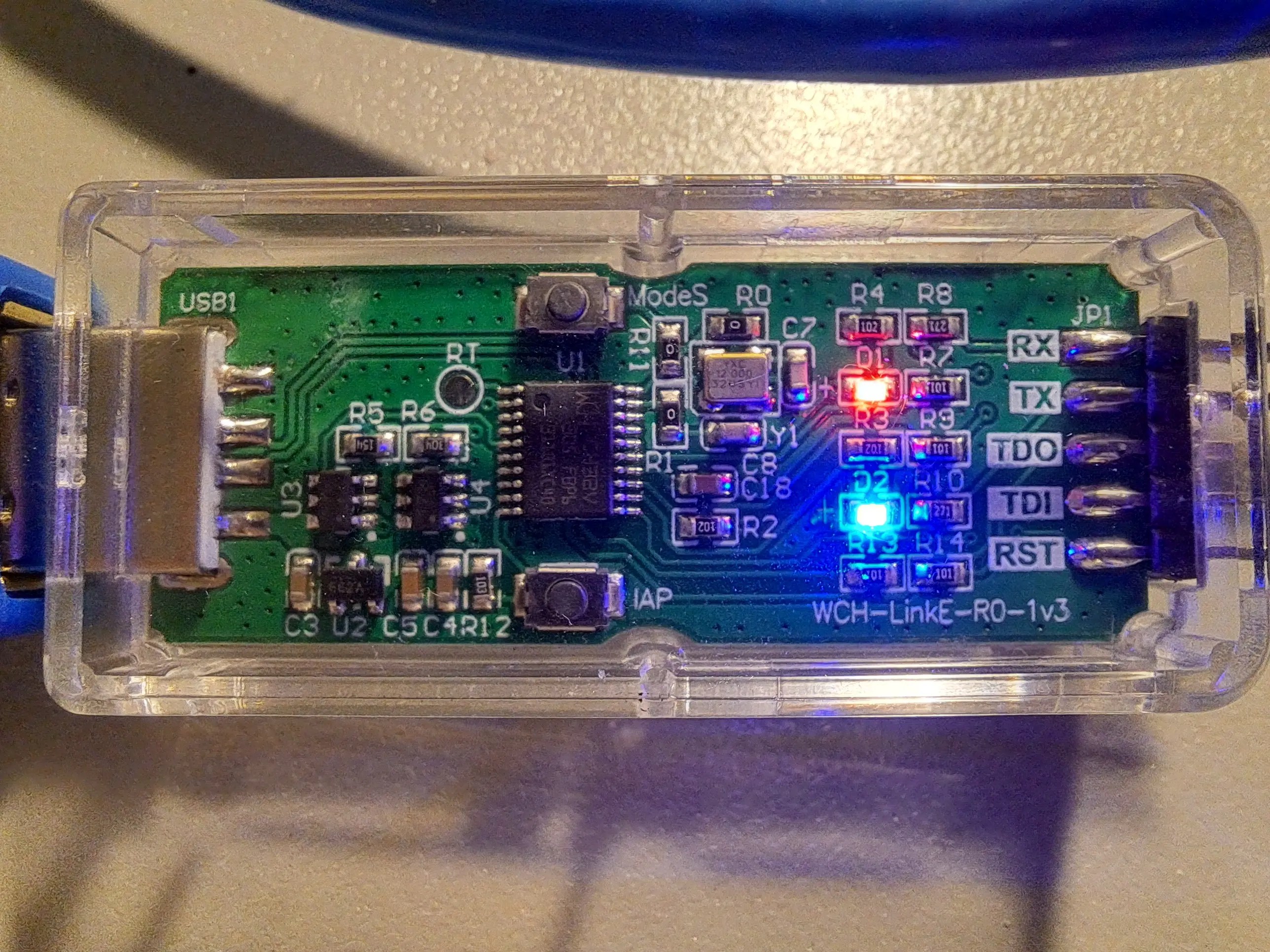
⚠ Warning. There are two similar programmers. The WCH-LinkE and the WCH-Link. You need the WCH-LinkE version. See the user manual.

If you intend to DIY, you’ll want the microcontroller, these are available from the manufacturer’s official AliExpress store:

If you intend to breadboard, you’ll also need an TSSOP to DIP adapter:

Or alternatively:

So many boards for $3.50

This minimal development board is compatible with both the CH32V006F8P6 and the CH32V003F4P6.

The PCB is panelized and V-scored, with 15 snap-off dev boards per panel. When ordered through JLPCB, you receive five panels—yielding a total of 75 boards—for about $3.50. That works out to just $0.046 per board.

Pair that with bulk pricing from the WCH Store (around $0.24 per microcontroller), and you’re looking at a complete dev board for roughly $0.30 each. It’s hard to beat that.

If you’d like to customize the design, you can also download the full EasyEDA project for the dev board and modify it to suit your needs.

If you don’t want to DIY a board. You can also buy a:

Schematic

The schematic is very straight-forward. The only truly critical component is the C1 decoupling capacitor. It must be placed as close to the chip’s pins as possible and have a solid ground connection. That’s difficult to achieve on a breadboard, which is where the dev board becomes especially useful.

To program the chip, you only need to connect GND and SWIO to the corresponding pins on the programmer — just two wires at minimum. If you’re powering the chip from the programmer, you’ll also need to connect VCC.

I’ve included a few optional conveniences that you can omit if desired:

  • A de-bounced reset switch
  • An LED on GPIO PD3
WCH-LinkE Programmer

The CH32V003/006 series is programmed using the proprietary WCH-LinkE programmer. This is a low-cost, single-wire programming interface that also supports single-wire debugging (SWD). The official programmer additionally includes a USB-to-TTL serial interface, which can be used to monitor debug output.

Programmer – Linux

If you are on linux. I’ve included some additional instructions here to setup PlatformIO IDE on VSCodium, and how to configure udev rules for the programmer.

Programmer – Windows

When you first plug in the programmer, you’ll probably see that there are missing drivers in device manager:

Programmer is missing the correct driver
  1. Download the driver from GitHub https://github.com/Community-PIO-CH32V/wchlink-driver-windows/archive/refs/heads/main.zip
  2. Install the driver in the folder WCHLink and WCHLinkSER. These are the drivers for the programmer, and the programmer’s inbuilt TTL-USB serial device
  3. Check device manager and expand both “Ports (COM & LPT)” and “Interface” in the tree. You should see that both the WCH-LINK SERIAL and the WCH-LINKRV devices are present.
Both drivers are working correctly.

Once you see both drivers are working correctly, you can move onto the next step.

Set WCH-LinkE RISC-V mode.

The programmer supports both an ARM and a RISC-V mode. If the programmer is in ARM mode, you will see a blue LED illuminated. That’s bad if you want to program the CH32V003/006

If there is no blue led, you can ignore the rest of this and go straight to setting up the programming environment.

Blue LED is lit, programmer is in the ARM mode. Not what you want to see.

If the blue LED is lit, you have to swap the mode. Luckily, you only have to perform this step once, as the mode will be written to eeprom.

There are three options I’m aware of to set the mode:

  1. Hold down the ModeS button while you plug the programmer into your USB port (Case can be a bit tricky to open though)
  2. Download the WchLinkUtility https://www.wch.cn/downloads/wch-linkutility_zip.html
  3. Use the python rvmode.py utility

I went with the WCHLinkUtility. Unzip and run WCHLinkUtility and then:

  1. Press Refresh
  2. Select WCH-LinkRV in the “Active WCH-Mode:” drop down
  3. Press Set

The blue led should no longer be lit, indicating the programmer is in the RISC-V mode. You can go onto the next step.

No blue LED is lit. The programmer is in the correct RISC-V mode.
Update Programmer Firmware

My programmer worked out of the box with the CH32V003, but for the CH32V006 I needed to fist update the firmware.

Programmer Firmware – Windows
  1. Open WCH-LinkUtility.
  2. Select the correct IC from the Series drop-down menu.
  3. Click Query Chip Info.

If a firmware update is required, the utility will automatically prompt you to perform it.

Updating WCH-LinkE firmware
Programmer Firmware – Linux

If you don’t have access to a Windows machine, you can use the open-source wlink-iap utility to update the firmware instead.

Connect the Programmer

Due to the SWD (Single-Wire-Debug) programming support. Only three wires are needed, and all are connected directly to the corresponding pins.

MicrocontrollerProgrammerSWIOSWIOVCCVCCGNDGNDRST (Optional)RST (Optional)

The programming wiring is so simple, it’s almost not worth this table.

Programming Environment

This setup is for the PlatformIO environment and the VSCode editor. There are options for Arduino IDE. But the PlatformIO solution is more mature, and debugging is supported out of the box!

Install PlatformIO Extension
  1. Open VSCode Extension Manager
  2. Search for official PlatformIO IDE extension
  3. Install PlatformIO IDE.
  4. Restart VSCode
Install PlatformIO from the VSCode extensions window
Add WCH32 support

Support for the WCH32 isn’t currently included by default with PlatformIO. This support needs to be added

  1. Select the PlatformIO icon (Ant head icon on the left)
  2. Select Quick Access -> PIO Home -> Platforms
  3. Select Advanced Installation
How to get to the Add Platform Wizard

Next, paste in the following URI:

https://github.com/Community-PIO-CH32V/platform-ch32v.git
PlatformIO Advanced platform installation screen

Press Install. If successful, you’ll be greeted with something like:

CH32 platform installed successfully
Create a new WCH32 project

Create a new project

  1. Select the PlatformIO icon (Ant head icon on the left)
  2. Select Quick Access -> Open -> New Project
The PlatformIO new project screen

In the new Project Wizard

  1. Enter a name ‘ch32-blink’
  2. Select board Generic CH32V003F4P6(W.CH) (Or the CH32V006F8P6(W.CH))
  3. Select the Ch32v003fun framework (It supports both the CH32V003 and CH32V006 series)
  4. Click finish
New Project Wizard Screen. Make sure you select the correct board

Ch32fun is a lightweight, bare-metal development framework for WCH’s line of microcontrollers. Ch32fun takes a minimalist approach—it gives you just the essentials (headers, tooling, and a single-file library) so you can work directly with the hardware registers as described in the chip’s Technical Reference Manual.

Add Code 1. Create a new file /src/funconfig.h

Add the following contents:

#ifndef _FUNCONFIG_H#define _FUNCONFIG_H// Place configuration items here, you can see a full list in ch32fun/ch32fun.h// To reconfigure to a different processor, update TARGET_MCU in the  Makefile#endif

funconfig.h is a per-project configuration header file that you create to customize how the ch32fun framework behaves for your specific application. It’s automatically included by ch32fun.h and serves as the main way to configure various system settings before the framework initializes.

We don’t need to configure anything now, but common settings you’d define in funconfig.h include:

  • FUNCONF_SYSTEM_CORE_CLOCK – Sets the target CPU clock speed (e.g., 48MHz )
  • FUNCONF_USE_DEBUGPRINTF – Enables fast printf debugging over the programming interface
  • FUNCONF_USE_UARTPRINTF – Enables printf over UART instead
  • FUNCONF_UART_PRINTF_BAUD – Sets UART baud rate (typically 115200)
  • FUNCONF_SYSTICK_USE_HCLK – Configures whether SysTick runs at full CPU speed or divided
  • FUNCONF_USE_CLK_SEC – Enables the clock security system
  • FUNCONF_DEBUGPRINTF_TIMEOUT – Sets timeout for debug printf operations
2. Create a new file /src/main.cpp

Add the following contents:

#include "ch32fun.h"#include <stdio.h>// use defines to make more meaningful names for our GPIO pins#define PIN_LED PD3int main(){    SystemInit();    funGpioInitAll();   // Enable GPIOs    funPinMode(PIN_LED, GPIO_Speed_10MHz | GPIO_CNF_OUT_PP);    // Set PIN_1 to output    while (1)    {        funDigitalWrite(PIN_LED, FUN_HIGH);        Delay_Ms(1000);        funDigitalWrite(PIN_LED, FUN_LOW);        Delay_Ms(1000);    }}

Remember to adjust the PIN_LED define for your board.

Upload

Click the upload button in the bottom right — you can also use the items in the Quick Access under Platform IO

The upload button hides at the bottom left

If everything worked you should see a green [SUCCESS] message and your LED will begin blinking.

Debugging

One of the most pleasant surprises about this chip is its fully featured debugging interface, supported over the same single-wire connection used for programming.

No additional setup is required to debug your project in real time. Simply set a breakpoint and click the menu item Run → Start Debugging.

A breakpoint will be hit at the very beginning of the project—ignore this and press continue. Your breakpoint should be hit next.

Excellent debugging facilities are supported out of the box

That’s it, congrats, you’re done!

Next Steps

For the next steps, I suggest checking out the examples included with the ch32fun framework. There examples demonstrate how to perform most common tasks on the CH32.

I also suggest reading the reference manual

https://siliconjunction.top/?p=2372
Extensions
A Very Low Cost GaN Charger For Your Bench.
Bench Tests6-port USB chargerbudget USB charger reviewelectronicselectronics lab bench powergearlow power USB chargermicrocontroller power supplymulti-device charging stationQuick Charge USB chargertechnologytravelUSB charger thermal performanceUSB multi-port chargerUSB PD 3.0 chargerUSB PD trigger testingUSB-C and USB-A charger
I often run a large number of USB devices on my lab bench—tablets, mobile phones, and various microcontroller projects. I also use a mix of USB-A and USB-C connections. Some older devices don’t behave correctly on USB-C ports due to misconfiguration, so having both types available is important. All of these devices are relatively low […]
Show full content

I often run a large number of USB devices on my lab bench—tablets, mobile phones, and various microcontroller projects. I also use a mix of USB-A and USB-C connections. Some older devices don’t behave correctly on USB-C ports due to misconfiguration, so having both types available is important.

All of these devices are relatively low power (under 20 W each), which makes high-cost, high-output chargers unnecessary. What I care about most is the sheer number of available ports.

Recently, I purchased a six-port USB charger from Amazon, and I’ve been impressed enough to share it. At only $24, it’s excellent value for a charger with this many non-shared outputs.

It’s actually the only charger under $25 that I’ve bought that hasn’t sucked in some way. This one seems to simply deliver exactly what was advertised with no frills.

Specifications
  • Three USB-A ports, up to 18 W each
  • Three USB-C ports, up to 20 W each
  • 100 W total combined output—effectively enough to run all six ports near full power
  • Supports USB PD 3.0 and Quick Charge
  • Output voltages of 5 V, 9 V, and 12 V (No 20 V support. 20 V is often used for laptop charging; this charger is aimed at lower-power gear)
Benefits
  • Each port is managed independently; connecting or disconnecting one device does not affect the others
  • Very low idle power consumption
  • Each port reliably meets its rated output
  • Excellent port count for the price
Downsides
  • Not a high-power charger: no 20 V output and a maximum of 20W per port
  • Ports can enter sleep mode when PD is not in use and current draw is very low — May be a minor annoyance to breadboarding projects. Saves both your money and the environment. See Sleep Mode for more details on this feature.
Parts Used
This sticker showing detailed specifications is underneath the charger, but no image of it existed on amazon.
Idle Power

This charger includes a low-power standby feature: when it detects that no devices are drawing power, it enters a sleep mode and reduces wall power consumption to nearly zero:

Idle power of the device is below what I can measure
Sleep Mode

I performed some testing as to exactly how the charger’s sleep mode works.

A small probe voltage is always present on each port, and as soon as the current exceeds a low threshold (around 10 mA), the port fully enables.

As tested with my PD trigger, any PD negotiation will automatically enable the port, so the sleep mode only affects “dumb” 5 V devices that don’t communicate over USB PD.

So In summary, the sleep behaviour is:

  • PD negotiation -> Port wakes up
  • Current draw above 10mA -> Port wakes up
  • Current draw dips below 10mA, and no PD negotiation present, port sleeps after about 10 seconds.
A small probe voltage is present on any sleeping ports

Most devices—phones, tablets, and similar—either negotiate USB PD or draw more than the minimum current, so the port effectively stays on while they are connected. I have seen a port enter sleep mode when very low‑power devices, such as a USB speaker, finish charging, but this hasn’t caused any issues.

I assume this probe voltage is a simple “Is this port in use?” detection scheme designed to reduce overall power waste for dumb devices.

The minimum load required to enable a port appears to be around 220–470 Ω (7–15 mA). If you want to keep a port permanently on for breadboard projects, a small resistor across the power rail will do the trick. Once you unplug your project, the port goes back to sleep—quite convenient.

With a 220Ohm or higher load present, this port will stay awake permanently.

Overall, the sleep mode seems like a useful feature if you don’t keep the charger in constant use, helping reduce unnecessary power draw. For general device charging, there’s no downside. For very small 5 V electronics projects, you may need to provide a modest minimum load to keep the port active.

Output Power Test

I set up a simple test to verify whether the charger can deliver its claimed output power. For this, I used an 8 Ω power resistor as a dummy load. At 12 V, the resistor should draw 1.5 A, resulting in a power draw of 18 W (12 V × 1.5 A), which is essentially the charger’s maximum per-port output.

Dummy load used for the power test

Using a PD trigger, I tested all available voltages—5 V, 9 V, and 12 V—and each was delivered successfully, as confirmed by the USB tester’s voltage readings and measured power into the load.

I then selected the maximum voltage of 12 V, connected the dummy load, and let it run for 30 minutes to check for any heating or voltage drop issues.

At close to full output power, there’s minimal voltage drop

After 30 minutes, the charger remained cool to the touch (the same could not be said for the dummy load), and the output voltage was a stable 11.93 V. That’s less than a 0.1 V drop—impressive performance for such a low-cost device.

Sound

Since some readers were curious, I tested the charger for any annoying sounds at full load by pressing my ear to it. The result? Complete silence—another green tick for this budget-friendly device.

Conclusion

This six-port USB charger appears to offers excellent value for low-power lab and bench use. It provides a high port count with a mix of USB-A and USB-C outputs, reliable per-port power delivery up to 20 W, and efficient power management with very low idle consumption. While I haven’t comprehensively tested all ports at their maximum output simultaneously, charging two tablets and a phone at the same time showed Rapid Charging active on all devices, and the charger remained cool to the touch.

Testing also confirmed it can sustain near-maximum per-port output without overheating or significant voltage drop. Although it lacks 20 V support for high-power devices, it’s a solid, inexpensive option for charging and powering multiple medium sized USB devices simultaneously.

https://siliconjunction.top/?p=2321
Extensions
A Simple, Battery-Free Guitar Input For Your Soundcard
AudioBeginneraudio interfacebeginner electronicscomputer audiodiydiy electronicselectronicsengineeringguitar bufferguitar electronicsguitar preampguitar recordinghome recordingmicrophone inputmusic productionrecording guitarsciencetechnology
If you’ve ever tried plugging a passive guitar straight into a computer soundcard, you might have noticed that it sort of works… but the signal is low, the tone is flat, and moving your guitar’s controls can sometimes do weird things. Typical solutions are USB sound interfaces, or dedicated preamps — like the more advanced […]
Show full content

If you’ve ever tried plugging a passive guitar straight into a computer soundcard, you might have noticed that it sort of works… but the signal is low, the tone is flat, and moving your guitar’s controls can sometimes do weird things.

Typical solutions are USB sound interfaces, or dedicated preamps — like the more advanced amplifier I built in this previous post, which uses a modern CMOS op-amp to drive line-level inputs. That circuit works anywhere but, of course, needs a battery.

This new, simpler buffer is different: it doesn’t provide gain or line-level output, so it only works with microphone inputs. But the advantage is that it runs entirely from the small bias voltage already present on your soundcard, no batteries required.

The Problem: Plugging Directly into a Mic Input

Many consumer soundcards provide a small DC bias voltage on the mic input. This is not phantom power (+48 V), but a tiny voltage (typically 2.5–4 V at 0.5–2 mA) intended to power electret microphones. I’m going to try to leverage it to amplify the current from my guitar.

Before building this project, make sure your sound card provides a DC bias. You can check this by setting your input to microphone and measuring between the sleeve and ring of the input jack with a multimeter. If you read a few volts or more, your sound card should be compatible with this project.

The 3.9V bias voltage on my realtek soundcard
The 1.4mA short circuit bias current on my realtek soundcard

If you plug your guitar straight in, you may run into issues:

Tone degradation
The tone can sound flat, dull, or lifeless. Passive guitar pickups are designed to drive a high-impedance load, but most consumer mic inputs present a much lower impedance — typically 600 Ω to 2 kΩ.

When you plug a guitar directly into such an input, the pickup and input form a voltage divider. Combined with the inductance of the pickups, this creates an RC low-pass filter, rolling off high frequencies and muting the signal. In my testing, the signal was technically usable, but it sounded like the guitar’s tone knob was permanently turned all the way down.

Control weirdness
Your volume knob, pickup selector, or coil-split switches can act unpredictably. Turning the volume knob may produce scratching noises, certain positions may trigger bursts of noise, and switching pickups can cause sudden jumps in volume. This happens because DC from the mic input flows through the guitar’s controls — something they weren’t designed for. It’s also affected by the fact that switching pickups or coils changes the guitar’s output impedance; when connected to the relatively low-impedance mic input, this can cause the signal amplitude to vary unexpectedly.

Even when the tone seems okay, the behavior of your guitar can be unstable — which makes recording or playing through software frustrating.

The Solution: A Simple JFET Buffer

A tiny JFET stage fixes all of these problems. It:

  • Blocks DC from reaching the guitar, so controls behave normally
  • Presents a high impedance to the pickups, preserving tone
  • Outputs a low-impedance signal that the mic input can handle
  • Runs entirely off the mic bias voltage, no batteries needed

The result? The guitar sounds exactly like it’s supposed to, the tone comes alive, and the controls work predictably.

Parts you’ll need

Note — Many JFETs sold on AliExpress/Amazon are fake. These suppliers have worked for me (Chanzon on aliexpress), but be wary, consider a more reputable distributor such as Mouser, DigiKey, LCSC.

You’ll also need either:

Or a

Schematic
The final circuit only requires six components.
Ground should be connected to the mic, guitar, and case

How It Works

This circuit is a JFET buffer, also called a source follower. It doesn’t amplify the voltage of your guitar signal — that stays roughly the same — but it does increase the available current. With more current available, less voltage is lost across the soundard’s microphone input.

High-impedance input for the guitar: The JFET gate draws virtually no current, so your pickups see a very high impedance. In this circuit, the input impedance is set by R2 to about 1 MΩ

Low-impedance output for the soundcard: The signal comes from the JFET source, which is dominated by R3. This gives an output impedance of roughly 3.3 kΩ, low enough for a mic input to handle cleanly without tone loss.

DC blocking: The gate is isolated from both the source and drain, so no DC voltage reaches the guitar.

Even if your soundcard happens to behave well without a buffer, this circuit guarantees consistent tone and control behavior across different devices, thanks to the defined input and output impedances.

Choosing Capacitors for This Circuit

This is a very simple circuit, but capacitor choice matters more than you might expect — especially in a high-impedance audio path like this one.

Ceramic (MLCC) Capacitors

Multilayer ceramic capacitors are small, cheap, and will last forever, but many common types (such as X7R and X5R) are microphonic. In my first build I used a 10 µF X7R capacitor in the signal path (C2). Electrically it worked fine, but the circuit is microphonic — tapping the enclosure produced clearly audible noise.

Verdict: Avoid X7R/X5R ceramics in the signal path. (C0G/NP0 types are fine electrically, but usually not available in large enough values.)

Liquid Electrolytic Capacitors

Standard electrolytics are easy to find and generally behave well in audio circuits. They are not microphonic, but they do have two downsides:

  • They must be installed with the correct polarity
  • Over very long periods (many years), they can dry out

If you use an electrolytic capacitor, choose a sensible voltage rating and double-check the polarity. The soundcard’s mic input sits at a higher DC voltage due to its bias supply, so the positive terminal of the capacitor should be connected on the soundcard side.

Verdict: Perfectly acceptable and beginner-friendly if used correctly.

Tantalum Capacitors

On paper, tantalums look like a good fit: compact, stable, and available in useful values. In practice, they performed poorly in this circuit. The leakage current was high enough to disturb the bias point, pulling it toward ground and preventing the JFET from biasing correctly.

Tantalums are also extremely sensitive to polarity — even a brief reverse-voltage event can permanently damage them and increase leakage.

Verdict: Not recommended for this project.

Solid Aluminum (Polymer) Capacitors

Solid aluminum polymer capacitors should also work very well here. They are:

  • Non-microphonic
  • Very low leakage
  • Long-lived
  • Happy at low voltages

While I didn’t use one in my own build, their electrical characteristics make them an excellent choice for this application.

They’re less likely to be lying around in a junk box, but if you have them, they’re ideal. If you’re buying new parts specifically for this project, this is the type to get.

Verdict: Best choice if available.

Construction

Due to the simplicity of the circuit, I decided to make the PCB by cutting islands into a scrap piece of bare board. This circuit only has four nodes plus ground, so I could lay them out in a simple two-row grid: four nodes along the top for the circuit, and a single row along the bottom dedicated entirely to ground.

Don’t judge me. I was free-handing a dremel
My populated PCB — microphonic ceramic capacitors and all. I used SMT resistors here, but through-hole parts work just fine too.

Note: When building this circuit, it’s likely simpler to connect the tip and ring (L and R) of the microphone together, this increases the available bias current, and means you don’t need to deal with separating channels when recording.

Enclosure

Because this circuit presents a high-impedance input, it can pick up tiny currents from ambient noise. For that reason, a metal case is practically mandatory.

Make sure the circuit has a good electrical connection to the case, and if possible, the panel-mount audio connectors should also make solid contact with the enclosure. This helps shield the circuit from interference and keeps your recordings clean.

Installing the pcb into the case. I 3D printed a small sleeve to give the case more support, and to prevent shorts.

I used a small metal tin from a local discount store — originally intended for cigarettes. I sanded off the original decoration and gave it a fresh coat of spray paint to make it look nicer. Simple, cheap, and effective.

Results

Here’s a sample recorded directly from the buffer using my Realtek onboard soundcard. I’m very happy with the results: the noise is low, and the tone is clear and bright.

Please forgive my amateur playing — I’m just a beginner! The point here is the circuit, not my chops, and it shows that even a simple, battery-free JFET buffer can deliver a clean, usable guitar signal.

As an added bonus, turning up the guitar’s volume can slightly overdrive the buffer, producing a warm, tube-like overdrive.

It’s subtle and gives a bit of vintage character, without harshness or extreme fuzziness.

Here’s a quick recording:

Post your build photos or questions below!

FAQ

Q: Should I put a 10 kΩ or 20 kΩ resistor in series with the gate to protect against ESD and static shock?
A: Yes — that’s a great idea. The resistor helps limit current into the gate and dissipates the energy from a static discharge, protecting your JFET from damage.

Q: There’s a lot of noise when I use this. What can I do?
A: Try lowering the input resistor R1 to 500 kΩ or 330 kΩ. This may slightly reduce the treble, but it should dramatically lower noise. Experiment to find the best balance between tone and noise for your setup.

Q: Can I use a different JFET?
A: Yes. Many small-signal JFETs marketed for microphone preamps will work fine. Just make sure it’s a typical low-noise N-channel JFET.

Q: I only get audio out of one channel.
A: Try soldering the tip and ring (left and right) of the connector together. This will feed the buffer output to both channels and give you a mono signal on stereo inputs.

Q: How do I make sure that the circuit does not draw more current than the audio interface can safely provide?

A: There’s no risk of damaging your sound card. The internal bias resistor in the soundcard limits the current to a tiny value, so the sound card remains safe—even if there were a dead short present.

In my testing with various onboard Realteks, USB sound cards, and Intel audio, all provided about 3–4 V at 1 mA on the mic input, which is more than enough for this circuit.

If you have a multimeter, you can test your sound card to confirm it can supply at least 0.5 mA.

Normally, the circuit draws only about 0.3–0.4 mA, since it presents a DC impedance of over 6.6 kΩ. This is well within the limits of a typical sound card mic input, so in most cases, you don’t need to worry.

If there is a problem, you might notice clipping or very low gain. You could double all resistor values to reduce current, but increasing them too much can make the JFET operate poorly and cause distortion, meaning the circuit might not function on some sound cards.

Because the circuit is cheap and quick to build, the simplest approach is just to try it.

Download audio
Download audio
https://siliconjunction.top/?p=2271
Extensions