This post is going yet another part in the DIY camera projects which have been doing since quite some time. In this post I will showing you next successful implementation of making C mount high lens mount USB C camera. This implementation will have absolute modular boards having dedicated Sensor board which can be changed if needed.
2.JPG)
24.JPG)
 Project Video
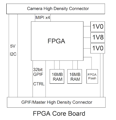
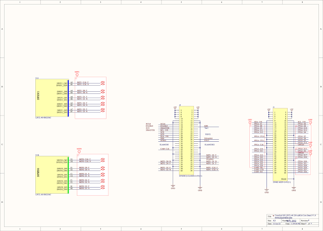
Hardware SystemThere are three boards, USB, FPGA and Sensor board. Sensor board has Sensor itself along with its power and Oscillator, Board has High Density connector to be able to connect to FPGA/Host board, High Density connector also supply power to the board has I2C, 4Lane MIPI with clock , I2C and also few other control signals.

FPGA board has in this case Lattice Crosslink NX LIFCL-40 in 256caBGA package with required power regulators, This board also has 2x 16Mybte RAM for applications that need additional memory, FPGA config flash memory is also on this board this board has two high density connector. Board pass I2C signal from Host right threw.
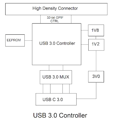
USB Board in this case has CYUSB3014 USB 3.0 Superspeed controller, along with required power and Memory, As this board has 3.0 USB C connector, so there is USB 3.0 mux is also there to support connector reversal
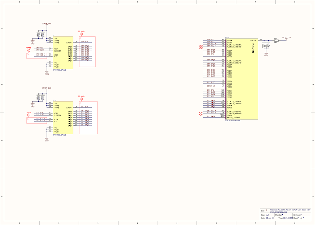
 Schematic
 Currently I have just one camera PCB, This schematic shows IMX290 IMX327 IMX462 PCB , all these 3 sensors have same resolution and also same PCB footprint.
 FPGA board


 USB 3.0 board


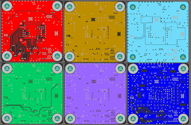
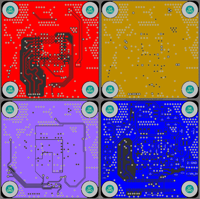
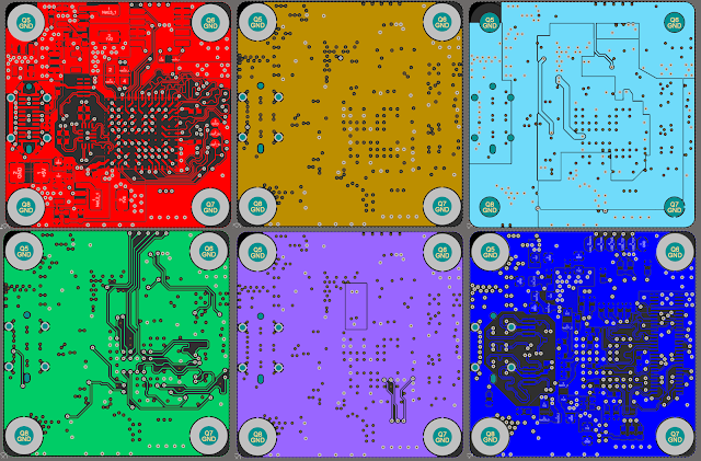
 PCB Boards
.JPG)
All of the boards are 6 Layer, All of them are 27 x 27 mm , while mounting holes are 22 mm appart
Camera sensor Board
.JPG)
 IMX477 Sensor PCB

FPGA PCB
.JPG)
 USB 3.0 Board
.JPG)
 Assembly
 1.JPG)
1.JPG)
2.JPG)
.JPG)
.JPG)
.JPG)
.JPG)
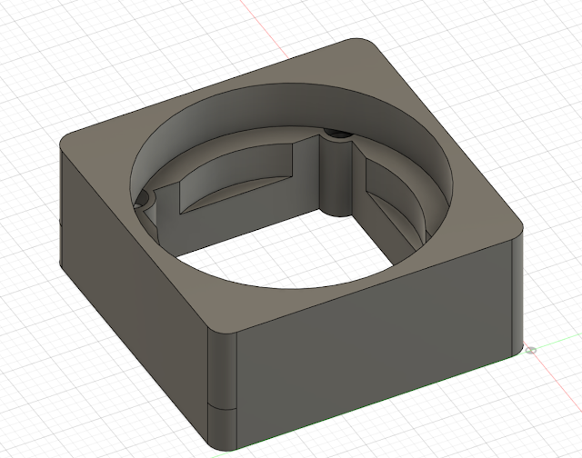
Hardware and Camera Lens C mountTo be able to mount a C mount lens I designed a mount in Fusion 360. as small threads on FDM printer are little hard to deal with There are many already made aluminum CS mount to C mount adapters are available online, Raspberry Pi camera also comes with one such ring, I bought these CS to C mount ring and I designed part around my PCB to fit these CS mount adapter ring to give me metal thread.
.JPG)
.JPG)
.JPG)
.JPG)
.JPG)
.JPG)
.JPG)
.JPG)
.JPG)
.JPG) Enclosure
Enclosure.JPG)
.JPG) FPGA Design
FPGA Design
MIPIWhat is MIPI, you can google it to find out but basically it is a interface specification for Displays and Camera sensor to a application processor.
Image blow show block diagram of MIPI. On one side there is application processor and other side is the peripheral. When peripheral is Camera and CSI apply. though mipi is closed specification which means one has to be member of MIPI consortium to gain access to full specification. And membership of the consortium comes with a big price tag for individuals. Luckily full specification is already available just a right keyword web search away. DCS, CCS, DSI, CSI and DPHY all the specification are available with just few minutes of web search.
 MIPI DPHY Signal
The image shows i got from google shows signal level for MIPI , HS driven by differential driver swings -200mV to +200mV at offset of 200mv. while LP signal is a 1.2V lvcmos

there are two different modes of transmission , HS mode and LP mode, HS mode is for hi speed display data while LP mode is for Low power transmission.
Receiver must detect when transmitter has gone into HS mode and exited HS mode.
Image blow shows how transmitter enter HS modes.

Stage 0 : LP-11 state in the shown image is LP state.
Stage 1 : To get into HS mode driver drives LPdp low for Tlpx(minimum 50ns) and stay in LP-01 (HS driver is tristate in LP 01).
Stage 2: Driver drives LPdn low for Ths-prepare (minimum 95ns) stay in LP-00 , Later somewere in the middle of this stage target device will activate it's 100R termination register.
Stage 3: Now Target is in HS, driver activates HS driver start sending mandatory zeros .
Stage 4: Send mandatory 0xB8 sync byte and then payload.
CSI
As explained earlier CSI , describes Packet structure. How exactly bytes are packed on to wire in different lanes configuration.
Image blow shows packet structure.

There are Two types of Packets
Short Packet: 4 Bytes (Fixed Length)
Long Packet: 6 - 655541 Bytes (Variable Length)

MIPI Short Packet Structure

MIPI Long Packet Structure
Endianness
Bytes are sent lsbit first and bytes in the packet are sent LSByte first.
 CCS
CCS
Very important fact with CCS when comparing with DCS , CCS describes command interface to be I2C while with DCS commands are set over same HS line as the data itself.
But in case of camera as per MIPI spec CCS is implemented over a extra I2C line.
CSI Single Frame
Single Frame from camera is show in the image blow.
Camera send a Frame start packet
Then send embedded line information which tells receiver about the stream
Then image data line by line.

Test Video
What make this camera sensor different to camera modules
IMX219 camera is bare bone camera sensor. What do means when i say bare bone camera sensor is , there not much image processing going on on the camera die it self. Camera sensor is Sensor array with Bayer filter on it , 10 bit ADC , clock system , MIPI output driver and I2C controllable system control.
What does this means for us as camera sensor implementer. As my final goal is to interface this camera to USB3.0 UVC with RAW YUV. This camera does not output YUV, forget about YUV this will not even output RGB. Camera output is absolute RAW 10-bit ADC conversion result from the Bayer filtered sensor array.
So go first get RGB output from bayer raw data, a Debayer or demosaic need to be performed. Once demosaic is done we will have RGB ready to be converted to YUV. And one we have YUV it can be transmitted to USB to be displayed.
What next this camera will not have is any automatic control over exposure. because camera does not have any intelligence to know how dark or bright scene is. Solution to this problem what raspberry pi implement is , Raspberry Pi regularly on each frame update analog gain register over I2C to adjust gain according to how bright and dark scene is.
This camera does not have any white balance control as well so host must do correct while balance compensations. To get correct colors out of image.
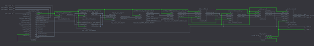
FPGA module Block Diagram
FPGA block diagram is show in the image blow. This diagram describe how overall system is implemented and what the key components what this diagram does not describe is control signals and other miscellaneous stuff.

Byte Aligner Received Raw unaligned bits from DDR RX module outputs Aligned bytes, Bytes on MIPI lane does not have any defined byte boundary so this modules Looks for always constant first byte 0xB8 on wire, once 0xB8 is found, byte boundary offset is determined, set output valid to active and start outputting correct bytes stays reset when data lane are in MIPI LP state .
Lane Aligner Receives multiple lane, byte aligned data from mipi rx byte aligner @mipi byte clock outputs lane aligned data in a multi-lane mipi bus, data on different lane may appear at different offset so this module will wait till of the all lanes have valid output start outputting lane aligned data so byte x from all the lanes outputted at same timescale
MIPI CSI Packet Decoder Basically a packet Stripper, removes header and footer from packet Takes lane aligned data from lane aligner @ mipi byte clock looks for specific packet type, in this case RAW10bit (0x2B) RAW12bit (0x2C) RAW14bit (0x2D). Module outputs Stripped bytes in exactly the way they were received. This module also fetch packet length and output_valid is active as long as input data is valid and received number of bytes is still within the limits of packet length.
MIPI CSI RAW Depacker Receives Upto 4 lane raw mipi bytes from packet decoder, rearrange bytes to output upto 8 pixel upto 16bit each output is one clock cycle delayed, because the way, output_valid_o remains active only while chunk is outputted
Debayer / demosaic Takes upto 8x upto 16bit pixel from depacker module @mipi byte clock output upto 8x upto 32bit RGB for each pixel , output is delayed by 2 lines Implement Basic Debayer filter, As debayer need pixel inform neighboring pixel which may be on next or previous display line, so input data is written onto RAM, only 4 lines are stored in RAM at one time and only three of the readable at any give time , RAM to which data is written to can not be read. First line is expected to BGBG , second line GRGR Basically BGGR format
RGB to YUV Color Space Converter Received upto 8 pixel RGB from the Debayer filter output upto 8pixel yuv422 Calculation is done based on integer YUV formula from the YUV wiki page
Output reformatter Takes upto 8pixel yuv input from rgb2yuv module @ mipi byte clock outputs 32bit 2pixel yuv output @output_clk_i , This block has RAM to have output clock independent of mipi clock, Output clock_clock must be fast enough to be able to get whole line worth of data before next line starts, This implementation of Output reformatter outputs data which which meant to send out of the system to a 32bit receiver depending on requirement this will be need to be adapted as per the receiver
Debayer / demosaic Need little more attention than other modules , IMX219 datasheet incorrectly mention output as to be either GBRG or RGGB.
But after wasting lots of time it turned out camera output BGGR . IMX219 Camera only output BGGR as defined by the IMX219 Driver in linux repo MEDIA_BUS_FMT_SBGGR10_1X10, Camera datasheet incrorrectly defines output as RGGB and GBRG. Data sheet is incorrect in this case.
To test my debayer, Iwas using built in camera test patterns. One key thing about IMX219 is Bayer filter type does affect test pattern as well. It seems like in Test pattern mode it outputs RGGB instead of BGGR. Test pattern will have R and B channel inverted when image have right color.
Update: I have discussed this issue with raspberry pi , It turned out flipping image seems to be the solution, once image flipped bayer output it correct for both data from sensor and test pattern. because flipping image does not affect bayer order of the test pattern.
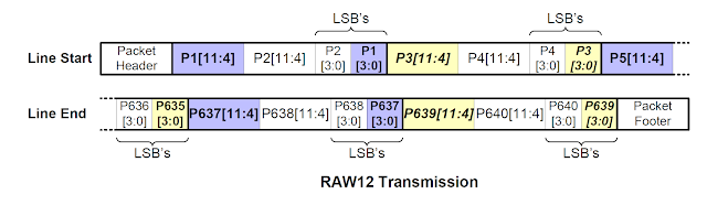
 MIPI RAW Packet Format

 ISP Pipeline Specifications
No virtual restriction on supported frame rate or resolution. Tested more than 4K with IMX477 4056x3040. Can do 8K with around 30FPS or even higher than that as long as FPGA is fast enough for needed frame rate and FPGA/Board has enough memory to be able to store minimum 4 Line worth of pixels. Output Clock is independent of MIPI clock. Easily Portable code to Xilinx or any other FPGA, No Vendor specific components has been used except for the PHY itself which can be replaced by other vendor's DDR phy and Embedded Block RAM. Only Debayer/Demosaic and Output reformatter need Block RAM. Block ram can also be replaced vendor's RAM. Auto detection of RAW pixel width supporting different camera sensors and sensor modes without FPGA reconfiguration.
Speed- Supports MIPI bus clock 900Mbitsps Per lane with upto 4 Lanes, Total 3.6Gbitsps Sensor bit stream, Has been Tested upto 900Mbitsps with 8x Gear.
- Pixel Processing pipeline with 2,4 or 8 Pixel per clock can reach more than 110Mhz with Lattice Crosslink-NX LIFCL-40 High Speed, So basically Can process upto 880 MegaPixels per second. With this can reach Around 120FPS with 4K resolution and around 30 FPS with 8K. Or even 3000 FPS with 640 x 480 as long as Camera and MIPI Wire allows. With Different Faster FPGA speed will be more.
- FPGA Oputput Pipeline is decoupled from MIPI clock, runs on output clock, It feeds into Cypress FX3 32bit GPIF can do Max 160Mhz. Cyress FX3's specs limits max GPIF clock to 100Mhz.
Configurability- Selectable max RAW pixel width
FPGA Design is configurable with parameters to support pixel depth from RAW10 to RAW14 or Virtually any bit depth even 16bit RAW when it becomes a MIPI Specs. Parameter specify maximum pixel width that is supported while module auto detect package type at runtime with RAW14 selected as max pixel width, RAW10, RAW12 and RAW14 will be automatically detected and processed
- Selectable number of MIPI lanes: With just definition of Parameter value number of lane is also configurable between 2 or 4 MIPI lanes.
- Selectable Pipeline Size: Pipeline is Configurable with a parameter to Process 2,4 or 8 Pixel. 2 Pixel Per Clock is only available with 2 Lane MIPI, while 8 Pixel Per Clock is only available with 4 Lanes.
- Selectable MIPI Gear Ratio: User can select weather to operate MIPI/DDR Phy in 16x or 8x Gear ratio. Most DDR/MIPI Phy supports 8x Gear while few do support 16x gear.
- Selectable MIPI continuous clock mode
User and select between MIPI clock lp based Frame sync or Frame start and frame stop packt based frame sync. Some MIPI cameras do not support going to LP mode while frame blank occur, With this option user can enable Frame Start and Frame stop detection, to have a frame sync. - Selectable ROM based Sample Generator
For ISP debuging ROM based sample generator can be activated. Two ROM lines are there have both even and odd line to full image test.
Block RAM and DDR PHY IPs need to be manually regenerated if Gear, pixel width , lane or PPC is changed.
Tests
4 Lane 12 bit IMX477 4056x3040 20 FPS Full Sensor 2028x1520 70 FPS Full Sensor Binned 2x2 2028x1080 100 FPS
4 Lane 10 bit IMX477 1332x990 200 FPS Binned 4x4 640x480 400 FPS Binned 4x4
2 Lane 12 bit IMX477 4056x3040 10 FPS Full Sensor 2028x1520 35 FPS Full Sensor Binned 2x2 2028x1080 50 FPS
2 Lane 10 bit IMX477 1332x990 100 FPS Binned 4x4 640x480 200 FPS Binned 4x4
2 Lane 10 bit IMX219 3280x2464 7 FPS 1280x720 30 FPS 1280x720 60 FPS 1920x1080 30 FPS 640x480 30 FPS 640x480 200 FPS 640x128 600 FPS 640x80 900 FPS
4 Lane 12 bit IMX290/IMX327/IMX462 1280x720 120 FPS 1920x1080 120 FPS
2 Lane 12 bit IMX290/IMX327/IMX462 1280x720 60 FPS 1920x1080 60 FPS
What decides camera Max FPS
Camera timing is controlled by just a few registers which control Clock. Then every sensor has a maximum ADC sample rate to convert Pixel Value to Digital, Different camera sensors have fast or slow ADC. or even multiple ADCs. so you do simple division on what your ADC pump needs for the needed frame rate. Shutter open time is also user adjustable so that also affects frame rate. And Interface clock is also important, If ADCs faster than how fast interface can pump data out of sensor then you have an issue of FIFO full.
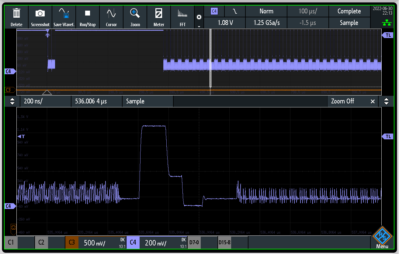
Scope capture
.png)
MIPI 2 Lane Mode, Decoded Data shows both lanes of lane aligned data IMX219 Full frame one of the line, on ch2 is byte clock
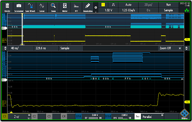
A start frame MIPI package (0x00), Use for Frame Sync with cameras where Clock does not go into LP during frame blank
.png)
A Frame Stop MIPI package (0x01) , Use for Frame Sync with cameras where Clock does not go into LP during frame blank
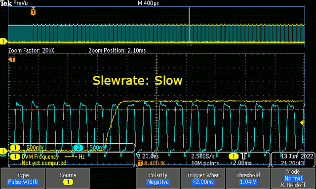
Show difference of Fast vs slow slew rate on GPIF port , CH1 shows GPIF port data line and ch2 is ~100Mhz clok
IMX477 Test pattern mode 0 were full is set to full 0x7FF and other colors are zero, but pixel where there is no blue color present shows high bits, Also Even line where there is no blue at all shows high bits, This must be kept in mind when matching colors
Test image
IMX219 Basic Test Full Frame Colors Uncorrected

IMX219 Full Frame Test pattern 5

IMX477 Full Frame Test Pattern 2
 IMX477 Full Frame Test Pattern 3
Cypress FX3 Firmware
Firmware implementation with FX3 was quite easy. I have put all the resolution and framerate in the USB descriptor , As described earlier this type of camera sensors are quite bare bone all the have sensor element, PLLs and ADC . So this camera sensor does not have any control over exposure, White-balance or even brightness, I have implemented manual control over USB UVC control channel. it possible to completely control camera exposure and brightness.
Few things you keep in mind, cypress fx3 clock frequency need to be set in 400Mhz mode to allow full 100Mhz 32bit GPIF DMA transfer.
One more thing is though Cypress CYUSB3014 has 512KB RAM but only 224 KB and additional 32KB is available for DMA buffer.
Having large buffer chunk is really important because on every DMA chunk CPU intervention is expected to insert UVC header. As this is high performance application less often CPU intervention is needed is better. So I have set DMA chunk / UVC individual packet to 32KB
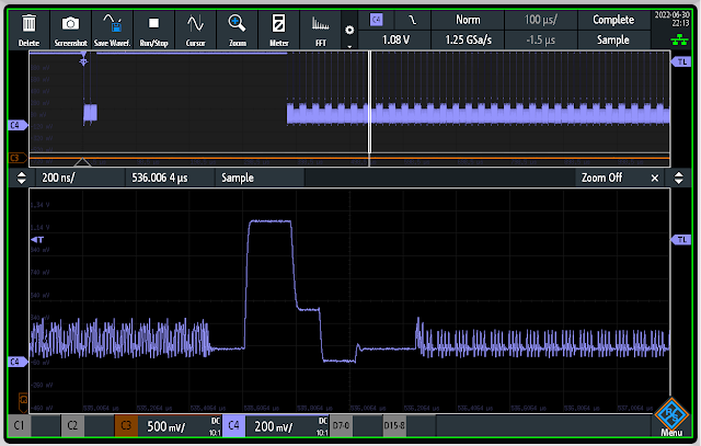
Scope capture Image blow shows Channel 13 is the individual DMA packet capture and on Channel 12 show CPU DMA finish interrupt.
These Two scope capture show difference between 16KB DMA vs 32KB DMA

16KB DMA Size, CH13 DMA packet , CH12 CPU interrupt

32KB DMA Size, CH13 DMA packet , CH12 CPU interrupt
PCB and Schematic Source is available in the Github Repo.
https://github.com/circuitvalley/USB_C_Industrial_Camera_FPGA_USB3.JPG)


.JPG) Top of the board Showing all 3 Ports and Indication LEDs
Top of the board Showing all 3 Ports and Indication LEDs.JPG) Back of the FMC Card Showing Power protection and Control Level translators
Back of the FMC Card Showing Power protection and Control Level translators .JPG)


.JPG) Top of the board Showing all 3 Ports and Indication LEDs
Top of the board Showing all 3 Ports and Indication LEDs.JPG) Back of the FMC Card Showing Power protection and Control Level translators
Back of the FMC Card Showing Power protection and Control Level translators .JPG)
.JPG)

.png)
.png)
.png)
.png)
.png)
.png)
.png)
.png)
.png)
.png)
.png)
.png)
.png)
.png)
.png)
.png)
.png)
.JPG)
.JPG)
.JPG)
.JPG)
.JPG)
.JPG)
.JPG)
4.JPG)
.JPG)
%20raspberry_pi_camera_fpga2.png)

%20raspberry_pi_camera_fmpga.png)
%20raspberry_pi_camera_fmpga.png)
%20raspberry_pi_camera_fmpga.png)
%20raspberry_pi_camera_fmpga.png)
%20raspberry_pi_camera_fmpga.png)
4.JPG)
.JPG)
.JPG)
.JPG)


11.JPG)
115.jpg)
115.jpg)
.JPG)
.JPG)
.JPG)

.png)
.png)


.JPG)


.png)
.png)
.png)
.png)
.png)
.png)
.png)
.png)
.png)
.png)
.png)
.png)


.JPG)
.JPG)


.JPG)
.JPG)
.JPG)
.JPG)
.JPG)
.JPG)
.JPG)
.JPG)
.JPG)
.JPG)

.JPG)

.JPG)
.JPG)


.JPG)
.JPG)

.JPG)
.JPG)


.JPG)
.JPG)
.JPG)
.JPG)

.JPG)
.JPG)
.JPG)

.JPG)
.JPG)
.JPG)
.JPG)
.JPG)

.JPG)
.JPG)
.JPG)
.JPG)
.JPG)
.JPG)
.JPG)
.JPG)
.JPG)
.JPG)

.JPG)

.JPG)
.JPG)
.jpeg)
.JPG)
.JPG)
.JPG)
.JPG)
.JPG)
.JPG)

.JPG)
.JPG)
.png)

.JPG)
.JPG)
.JPG)
.JPG)
.JPG)
.JPG)
.JPG)
.JPG)
.JPG)
.JPG)
.JPG)
.JPG)
.JPG)
.JPG)
.JPG)
.JPG)
.JPG)
.JPG)
.JPG)
.JPG)
.JPG)
.JPG)
.JPG)
.JPG)
.JPG)
.JPG)
.JPG)
.JPG)
.JPG)

.JPG)
.JPG)
.jpg)
.jpeg)
.JPG)
.JPG)
.JPG)
.JPG)
.JPG)
.JPG)
.JPG)
.JPG)
.png)
.JPG)
.JPG)
.JPG)
.JPG)
.JPG)
.JPG)
.JPG)
.JPG)
.JPG)
.JPG)

.JPG)

.JPG)
.png)
.png)


.png)
.png)
.png)
.png)
.png)
.JPG)
.JPG)
.JPG)
.JPG)
.JPG)
.JPG)
.JPG)
.JPG)
.JPG)
.JPG)

.png)
.png)
.png)


.png)
.png)
.png)
.png)
.png)
.png)
.JPG)
.JPG)
.JPG)

.JPG)
.JPG)
.JPG)
.png)
.png)
.png)
.JPG)
.JPG)
.png)
.png)
.png)
.png)
.png)
.png)
.png)
.png)
.png)
.png)
.png)
.JPG)
.JPG)
.JPG)
.JPG)
.JPG)
.JPG)
.JPG)
.JPG)
.JPG)
.png)
.jpg)
.jpg)
.JPG)
.JPG "Flap soldered back to Prevent sorting with Enclosure.")
..jpg)

..jpg)
.JPG)
2.JPG)
24.JPG)


.JPG)
.JPG)


.JPG)

.JPG)

1.JPG)
1.JPG)
2.JPG)
.JPG)
.JPG)
.JPG)
.JPG)

.JPG)
.JPG)
.JPG)
.JPG)
.JPG)
.JPG)
.JPG)
.JPG)
.JPG)
.JPG)
.JPG)
.JPG)


.png)

.png)