Documentation for the project shown at Hackaday Europe 2026 in Lecco. Link to paper pre-print: https://arxiv.org/abs/2603.18848 Find the KiCAD project for both 50 Ohms and 75 Ohms versions here (including […]
Show full content
Documentation for the project shown at Hackaday Europe 2026 in Lecco.
software hacks and fixesanalogAnalog DevicesexportLinear TechnologyLTmacromodelOpAmpOperation AmplifierreusesimulationSPICEsymbolTexas InstrumentsTI
This is a quick guide to gaining access to a large variety of TI parts – in particular operational amplifiers – in LTspice. We’re going to export the SPICE macro […]
Show full content
This is a quick guide to gaining access to a large variety of TI parts – in particular operational amplifiers – in LTspice.
We’re going to export the SPICE macro directly out of TI’s own SPICE tool “TINA” and import it to LTspice. This is non-intuitive, but once you’ve seen how it’s done it’s not so hard.
Both TINA TI and at least v17 of LTspice can be installed and run on Linux via WINE (just sayin).
Remember: THE SPICE MUST FLOW, in our case from TI to LT.
Step 1: Mining the SPICE
Option A: GUI
I assume you already have TINA (https://www.ti.com/tool/TINA-TI) installed. Open TINA and click on the register card “Spice Macros” then click on the OpAmp symbol on the left in the row just above.
Then select your desired part and place it on the empty sheet.
Right-click on the part and go to “enter macro”
A text editor will open, showing you the entire .SUBCKT definition of the OpAmp.
Select everything and copy it to clipboard. Paste it into your favorite text editor and save it as “opa355.lib” in the same folder as your LTspice project.
Option B: find the source files
Alternatively you can hunt for your SPICE macro manually in the installation files of TINA.
look in ~/.wine/drive_c/Program Files (x86)/DesignSoft/Tina 9 - TI/SPICELIB/
either the part you’re looking for has its own .lib file in this folder
or it is part of a .lib file with multiple entries
find it with grep
$ grep "OPA355" -R -H . ./Operational Amplifiers.LIB:* OPA355 SPICE Macro-model 03/01/02, Rev. 3 by Bill Sands ./Operational Amplifiers.LIB:* BEGIN MODEL OPA355 ./Operational Amplifiers.LIB:.SUBCKT OPA355 1 2 3 4 5 6
aha! So OPA355 is somewhere in Operational Amplifiers.LIB
Step 2: using the SPICE
In your LTspice project, place a new part – in the “Devices” list go to Operational Amplifiers and select the “opamp2” symbol.
Place a SPICE directive on the sheet and include your new SPICE macro file with the lib command:
.lib opa355.lib
Then right-click on the opamp symbol and give it the correct value (in this case “OPA355”), that is the name of the .SUBCKT in the macro file.
But before we run our simulation – we have to check if the pin order is correct!
meaning your SUBCKT has 5 pins and they are in the order (in+) (in-) (+V) (-V) (out), then you are good to go and can go ahead and run your simulation.
In the case of our freshly mined OPA355 we were not so lucky. The pin order was scrambled and we have an additional enable pin :(. But fear not we can make it fit:
* BEGIN MODEL OPA355* PINOUT ORDER 1 2 3 4 5 6* PINOUT OUT -V +IN -IN EN +V ***** original pin order*.SUBCKT OPA355 1 2 3 4 5 6***** new pin order!***** reorder pins to conform with LTSpice standard opamp pinout.SUBCKT OPA355 3 4 6 2 1***** enable input always high* new 100R resistor between pins/nets 5 (enable) and 6 (+V)R62 5 6 100[...]
You see I just reordered the internal nets (named “1”,”2″,”3″,…”6″) in the SUBCKT definition so they are in the same order as in the above example with our trusty TL082. And I left out net “5” which is the enable pin. I added the line “R62 5 6 100” which means “add an internal resistor of 100R that pulls enable (5) to +V (6)”.
Cool – now you can use OPA355 like any other OpAmp in LTspice – even if the SPICE code was “stolen” from the competing software product Enjoy.
hacksmusic related tech3D printingDIYeasyFreeCADfxguitarlow noisepower
Motivation Guitar effect pedalboards … If this post is for you, I guess I don’t have to explain this concept in great detail here. Most of us have a USB […]
Show full content
Motivation
Guitar effect pedalboards … If this post is for you, I guess I don’t have to explain this concept in great detail here. Most of us have a USB power bank lying around somewhere that can charge your phone or wireless headphones, should you end up somewhere without access to a wall outlet.
So you have a collection of your favorite guitar, bass or keyboard effect pedals, arranged nicely in a case – wouldn’t it be nice if you had something like a USB power bank to power your pedalboard on the fly, or at at a gig without needing to find a suitable outlet at the messy front of the stage?
Yeah? Read on
Complications
In principle a beefy regular power bank can deliver enough juice to keep your pedals running for a while. And I tried it out with mediocre success. Here’s why:
Power banks turn themselves off when you don’t draw a certain amount of current. If you only power a few analog pedals, like a tuner and a distortion stompbox, you may find that the power turns off after some tens of seconds.
USB power banks deliver 5V. Your standard pedals work with 9V – so you need a boost power converter which might generate some switching noise that might end up in the output. Also the power bank most likely has a boost converter in the first place to go from the battery voltage to 5V. So you have two switchers in a row. Meh.
Guitar pedals have power filter capacitors to keep the supply voltage nice and smooth and reduce power supply hum to a minimum. If several pedals are wired in parallel and you switch everything on at the same time, the resulting inrush current may trigger the overcurrent protection of either the built-in or the additional 5V to 9V boost converter. And then your board might not turn on at all, or worse – oscillate between off and almost on. Not cool!
The solution – Keep it simple, stupid
How about we use a power bank that already has several Li Ion cells in series and outputs a voltage greater than 9V? And it should easily charge with a USB-C jack. And handle the sudden inrush current. And never turn off. And while we’re at it – throw in a charge level indicator.
It’s a battery pack for the TRIXIG cordless drill. Conveniently you can buy an extra battery (15€ in Germany) without actually having to buy the entire drill.
The battery pack output voltage is (depending on charge level) something between 10 and 12.6V. Just wire a plain stupid 7809 voltage regulator between the battery pack and the pedal board and Bob’s your uncle.
More 3D printing – less electronics
Now we need something that can reliably attach to the battery contacts and houses the voltage regulator.
Usually I’m a fan of solving problems by clever use of electronic components. But in this case, less is more. So this ended up being more of a 3D design project. And a project to end my decade long boycott of FreeCAD. I designed my very first 3D printed part in FreeCAD back in 2013 or so and was utterly frustrated. Now (2025) I saw a colleague use it and decided to give it (now at v1.0!) another chance. It still crashes occasionally, but I was quite pleased with my finished parts:
First the bottom part. It features slits for the sheet metal contacts and rails to grip their counterparts on the battery housing.
Next a cover with mounting holes for M2.5 screws to attach to the bottom part, enough space inside for a mechanical toggle switch and a 7809 voltage regulator plus heatsink. Also some slits for ventilation.
Assembling everything is a bit fiddly but otherwise pretty straightforward. I advise you to first solder the wires to the metal contacts – it takes a while until the metal gets hot enough to properly join with the solder. When cooled, glue it into place with superglue (i also added filler granulate, alternatively fill the gaps with baking soda). I had no space to fasten the nut of the toggle switch – so I had to glue it into place as well – again making use of the superglue filler.
As you can see, the new power supply is almost exactly the size of a standard boss pedal, footprint and height
The battery pack easily snaps on and off. If you have a spare battery pack you can use one while the other recharges on your phone charger. Life is good.
analog projectsCFDcomparatorcomponentsConstant Fraction Discriminatordetectorelectronicsfast timingopen accessparticle detectorparticle physicsphotomultiplierphysicsPMTschematicsciencescintillatorTDCtechnologyvoltage
TLDR I built a relatively simple, cheap, and most of all maker friendly Constant Fraction Discriminator for high precision photomultiplier (and SiPM) timing applications. I wrote a paper about the […]
Show full content
TLDR
I built a relatively simple, cheap, and most of all maker friendly Constant Fraction Discriminator for high precision photomultiplier (and SiPM) timing applications.
I wrote a paper about the circuit, it was published open access (yay!), and now I hope you’ll read it
Motivation
When working with scintillation detectors and photomultiplier tubes (PMT) an often encountered problem is the so-called time-walk effect. This describes the phenomenon, that when evaluated with a comparator (or *discriminator*, as physicists like to call it), pulses of larger amplitude appear to arrive earlier than smaller pulses, because they surpass the comparator/discriminator threshold faster.
So even though your Scintillator and PMT might have an intrinsic timing precision of some 100 ps or less, the time-walk effect might reduce your signal timing quality to several nanoseconds.
Smart analog electronic tinkerers came up with a solution to this problem already back in the 1960s and they called it the “Constant Fraction Discriminator” (short CFD). The main idea is not to trigger on a fixed threshold but effectively trigger on a fixed fraction of each pulse’s amplitude.
I came up with a particularly simple and cheap implementation of the CFD concept, presented it at last year’s TWEPP24 conference (a CERN organized workshop on particle detector electronics) and wrote a proceeding paper about the circuit. The benefits of the circuit are best described by quoting from my own paper
Typical analog CFD circuits utilize multiple high-bandwidth operational amplifiers. Such devices must be able to operate up to 100 MHz or more, to reproduce the steep leading edge (few ns) of the detector signal. Suitable amplifier ICs tend to be costly and consume significant amounts of power. A specialty of the design proposed in this paper, is the complete lack of op-amps — to save power, costs and board space. Instead it employs only a handful of low-cost RF transistors in combination with differential LVDS receivers in place of analog comparators. Without sacrificing performance the heart of the circuit, the constant fraction shaper, was reduced to its most minimalist form, comprising only a single transistor and a delay line, apart from passive components. — (Michael Wiebusch 2024 JINST19 C12009)
… or in other words – my CFD approach is basically a weird RF hack which involves doing unconventional things with transmission lines
Also, my slides from the conference talk are still online, if you like -> click here to view
The paper describes the shaper in great detail and why this thing works at all. However, the space was limited and I could not present the full circuit with all the tricks I did with the LVDS receivers. But in this blog post I can. That’s why I present you …
The Full Circuit
Here you have a working prototype schematic in its full glory. The detailed discussion of the circuit is in the paper.
Performance
Apart from what was said in the paper, here is a nice and graphic performance demonstration:
Left: A pulser generated stimulus, closely imitating a LaBr scintillation crystal coupled to a PMT.
Right: The reaction of a simple leading edge discriminator (a.k.a. comparator) compared to the output of the presented CFD. While the input amplitude was varied over a factor of 10, the standard deviation of the logic output of the CFD is only 60 ps.
software hacks and fixesFPGAGHDLghdl-yosys-pluginlinuxmakeropen sourceoss-cad-suiteVerilogVHDLYosysYosysHQ
TLDR I discovered that YosysHQ’s oss-cad-suite now “secretly” supports code entry not just in Verilog but also in VHDL. (Update: well I looked at older releases and VHDL support was […]
Show full content
TLDR
I discovered that YosysHQ’s oss-cad-suite now “secretly” supports code entry not just in Verilog but also in VHDL.
(Update: well I looked at older releases and VHDL support was there for a long time already – it just was not obvious to me! And I still see a lot of blog and forum posts claiming that you need the commercial version of oss-cad-suite for VHDL.)
In this post I give a quick overview over the main components of the toolchain and show a quick and easy way to get an example VHDL project to compile.
Motivation
Over the past months I’ve become quite fond of the YosysHQ FPGA development toolchain. The best thing is: It’s completely open source! Of course not all FPGAs from all vendors are supported – but it’s great for makers to get started with some low-end low-price and low-power FPGAs like the Lattice iCE40 devices which were completely reverse engineered by project icestorm. Instead of installing a bloated IDE blob that is not guaranteed to work in Linux, YosysHQ offers you a set of command line tools that can be orchestrated with a humble makefile, thus you can go about your first FPGA adventures almost like compiling a C program.
The most important components (among others) of the YosysHQ toolchain are:
Yosys – the logic synthesis tool which maps your HDL code (in this case Verilog only) to logic gates
nextpnr – the automatic place and route tool
icestorm – the database of knowledge about all wires and logic cells inside the Lattice iCE40 FPGAs and tools to generate iCE bitstreams
openFPGALoader – a tool to program the bitstream (the “compiled” binary) onto your FPGA or it’s external flash IC
To spare you the hassle of installing all the bits and pieces yourself, YosysHQ offers a nightly binary prebuilt package: https://github.com/YosysHQ/oss-cad-suite-build . Just go to the release page, download the tarball for your system, extract it, set your environment variables and paths with “source environment” and you’re good to go – if you program your FPGAs in Verilog. If you wish to code in VHDL then you’re out of luck but you might consider buying YosysHQ’s commercial software bundle Tabby CAD Suite which does indeed support VHDL.
However the internet knows that you CAN get Yosys to work with VHDL input: There is a powerful open source VHDL simulator called GHDL which can be used as a VHDL “front-end” for Yosys via the “ghdl-yosys-plugin”. But you need to compile everything, icestorm, Yosys, nextpnr, GHDL and the ghdl-yosys-plugin from sources in the right order, so they are binary compatible and can all work in unison in the end. Which is quite tedious, there are many pitfalls, and there seems to be no good HOWTO to walk you through all the steps. GHDL, for example, is written in Ada, so you need to install an Ada compiler first. And the README files in the individual git repos are not necessarily all on the same page and often link to outdated documentation or to dead ends.
At this point I actually wanted to share my Docker container with you where I solved the problem once, so you don’t have to. But meanwhile there seems to be an even simpler solution:
I discovered that the oss-cad-suite includes the ghdl-yosys-plugin (and of course GHDL) by default! Someone must have added it recently (actually a while ago). They just don’t make a big deal out of it!
So how about we just try to see if we can build an iCE40 VHDL example project the quick and easy way?!
# download latest oss-cad-suite tarball
# today is Dec 2 2024
wget https://github.com/YosysHQ/oss-cad-suite-build/releases/download/2024-12-02/oss-cad-suite-linux-x64-20241202.tgz

# extract it
tar -zxvf oss-cad-suite-linux-x64-20241202.tgz

# enter directory and set environment
cd oss-cad-suite
source environment

# step out of the oss-cad-suite
cd ..

# now let's get the "hello world" blink example VHDL project from the ghdl-yosys-plugin repo
git clone https://github.com/ghdl/ghdl-yosys-plugin
cd ghdl-yosys-plugin/examples/icestick/leds/

# compile it!
make
If the end of your make output looks like the following :
analog projectsaudiocapacitorsdistortionelectronicsguitarlong-tailed-pairresistorssigmoidsynthesizertransistors
Motivation This is a very short one – but I felt like sharing this with the world. I was playing around with the humble long-tailed pair transistor amplifier in LTSpice. […]
Show full content
Motivation
This is a very short one – but I felt like sharing this with the world.
I was playing around with the humble long-tailed pair transistor amplifier in LTSpice. I noticed something interesting – not only can it be used as a differential voltage amplifier, but it seems it can also be used to implement a sigmoid function.
Wikipedia states : “A sigmoid function is any mathematical function whose graph has a characteristic S-shaped curve or sigmoid curve.”
Famous sigmoid curves are the logistic function or the error function. Most anything that is an integral of some bell curve becomes a sigmoid curve.
The circuit
Nothing special, we only have two npn transistors and three resistors. The base of the right transistor is kept at 1V, while the entire circuit is powered with 3V.
At the base of the left transistor we ramp up the voltage linearly, the output voltage is measured at the collector of the right transistor. With the chosen transistors, voltages and resistors we get the following beautiful behaviour:
What’s especially nice is that the center of the sigmoid is reached exactly when the left base is at 1V, just like the right base.
If you play with the voltage and resistor values you can change the sigmoid shape – not all choices keep the curve so nice, smooth and symmetric.
Variation: a gentler slope
If you wan the sigmoid to rise less abruptly then you can add a voltage divider at the left base as follows (The combination of R8/R7 could also be a potentiometer for a continuous trimming of the slope):
We get the following behaviour (blue curve: new circuit, red curve previous circuit)
What is it good for?
I don’t know
Here are some ideas:
Implementing neural networks with sigmoid activation functions – with discrete BJTs – haha joke
Guitar/synthesizer distortion or soft limiter sound effects? Someone try it out, I’m too lazy
Analog regulators that need soft limits of the controlled variable
Transforming linear synth CV signals into smoothly saturating non-linear parameters
Soft distortion idea:
The input/output signals are line-level AC signals
Effect on waveforms:
gain potentiometer set to high (80%)
gain potentiometer set to medium (50%)
gain potentiometer set to low (20%)
Synthesizer CV transformation idea:
Say we have a triangle wave synthesizer CV signal – what if we put it through the sigmoid transformation machine?
The output looks much more like a slightly distorted sine wave:
digital projectshacksmiscADCanalogreadarduinoDIYHacklow costmicrocontrollerpush buttonSPSTTrick
Motivation Sometimes you just barely get away with the number of available microcontroller GPIO pins to implement the desired functionality — And then you discover that you have no more […]
Show full content
Motivation
Sometimes you just barely get away with the number of available microcontroller GPIO pins to implement the desired functionality — And then you discover that you have no more pins left to read out any buttons that a user could push to actually operate the device.
What I present you now is a solution to get away with sacrificing just one µC pin and get four buttons in return without adding any additional digital (or analog) ICs.
You might have guessed it, it can’t be just any GPIO pin but it has to be an ADC pin. With a tiny trick the circuit even allows to correctly decode combinations of two buttons pressed simultaneously.
This technique is especially useful if you use an ATTiny85, i.e. you only have six GPIO pins to start with, but at least four of them can be used as ADC.
Not The Circuit
Okay, you say, that is simple – 4 buttons that is 4 bits of information = 16 different states which can easily be mapped equidistantly across the range of the ADC. A regular 10 bit ADC should have no problem distinguishing between those 16 different voltages. So far, so good.
a 4 bit R2R DAC
Maybe the schematic of an R2R-DAC pops into your mind – with buttons as digital signal sources at each stage (a0 … a3) of the resistor ladder – problem solv… oh dang – a regular push button can only actively pull low OR high (not both). Hmm. (But I bet this would work with SPDT switches!)
The Circuit
Let me propose something different instead:
a different kind of ladder
We even get away with six instead of eight resistors in comparison to the R2R ladder.
I guess you immediately get the basic idea: RA and R1..4 comprise a resistor ladder giving us four distinct voltage levels and by pressing one of the push buttons you select the respective ladder voltage to be measured by the ADC. RB is just a weak pull down, so the ADC sees 0V when no button is pressed.
“DUH!” – you say, “that’s not four independent buttons! I want to use key combinations.”
Okay at this point I have to admit: This will not give you the full 4 bit of button information, sorry. — However, if you like key combinations – ask yourself what is the maximum number of buttons you intend to push down at the same time? If you only need combinations of two buttons then this still is for you.
You see the ladder is not entirely symmetric. RA is 680R, while the rest is 1k. If they all were 1k then you could not distinguish between, for example, the combination SWA+SWD and the combination SWB+SWC, since both would produce close to VCC/2.
With RA different from the other ladder resistors we can actually resolve all ambiguities for combinations of one or two simultaneous button presses. The value of 680R is not the optimal value (750R) but it is close enough – and more importantly – part of the E12 resistor series. So you should have no trouble finding suitable resistors.
The Calculation
“So there are no ambiguities, but you made a complete mess with that crooked divider. What voltage corresponds to which button?! I don’t want to calculate that mess!” — okay I hear you. Look I already did the calculation (with a tiny python program) so you don’t have to. Here are the results:
or alternatively if we sort the configurations by voltage:
Or once again – grouped into zero, one or two buttons pressed:
The closest distance of two voltage values is 3.9% of VCC. Q: How do I know this is close to the optimum? – A: More brute force calculation in python.
Arduino Code
So we can get our button information back by implementing a lookup table in the Arduino code. In order for the measurement and the decoding to be robust I allow for a margin of error of ±3.9/2% from the theoretical ADC value (a value region 38 LSB wide). In the following table I assume we measure the voltage divider ladder with a 10bit ADC (typical AVR based Arduino).
Here is some Arduino code that will do the job – the lower nibble of the return value represents the buttons that are currently pressed. You might notice, that I only check the ADC value against the upper boundary, which is totally sufficient.
# in this example we have the buttons on A0
# change this to your ADC pin
const int button_adc_pin = 0;

uint8_t decode_adc_buttons(){

  int adcval = analogRead(button_adc_pin);

  if (adcval <= 100)
    return 0b0000;
  else if (adcval <= 253)
    return 0b0001;
  else if (adcval <= 294)
    return 0b0011;
  else if (adcval <= 398)
    return 0b0101;
  else if (adcval <= 451)
    return 0b0010;
  else if (adcval <= 569)
    return 0b0110;
  else if (adcval <= 625)
    return 0b1001;
  else if (adcval <= 667)
    return 0b0100;
  else if (adcval <= 778)
    return 0b1010;
  else if (adcval <= 848)
    return 0b1100;
  else if (adcval <= 888)
    return 0b1000;
  else
    return 0b0000;
}
Some more thoughts
Can you do five buttons on one pin WITH combinations of two? – I quickly simulated that, but It does not look promising. Too many combinations too close together. But hey, if you got two analog pins to spare, you could get already eight buttons!
“Help, I have a microcontroller with a 12 bit ADC, how can I use this method?” – Divide the result of the analogRead by 4. Then you have effectively a 10 bit ADC.
“It’s almost working but sometimes I get weird results. Some buttons seem to trigger the functions of other buttons?!” – Just like digital buttons bounce, our analog button ensemble can “bounce”. By that I mean trying to decode nonsensical data when the ADC reads the voltage while the µC pin is in the middle of being charged (or discharged) to the target voltages of the divider. Just like with digital bouncing you can de-bounce the output of “decode_adc_buttons()” by calling the function twice or more and check if a “button” (a bit of the function’s return value) transitions from LO to HI and stays HI for a certain number of cycles or milliseconds. Et voila.
analog projectsmusic related tech400074xxbeat frequencyCMOSDIYfx pedalguitarring modulatorsound effectstompbox
Demo Video Introduction Earlier this year I wrote a post about how to build a simple shortwave receiver with nothing but widely available hobbyist electronics parts, i.e. 74HCxx ICs, standard […]
Show full content
Demo Video
Introduction
Earlier this year I wrote a post about how to build a simple shortwave receiver with nothing but widely available hobbyist electronics parts, i.e. 74HCxx ICs, standard transistors and op-amps. Half-jokingly I called it “a 74xx defined radio“. The heart of the receiver is a 74HC4051 analog switch that I use as a (slightly unorthodox but cheap and easy to use) HF mixer.
Now I’m going to present you almost exactly the same circuit (or at least a part of it), working in the exact same way as in the radio, but instead of an antenna, we’re going to plug in an electric guitar. The goal is to make the guitar sound weird. Something like a ring modulator effect.
The PCB you can see in the video was actually designed for the 74xx receiver but now has only half the components assembled :). Of course you can build the circuit just as well on normal protoboard.
Schematic
If you compare this with the schematic of the shortware receiver, you will find out that I threw threw away the second half of the circuit (IF filter and demodulator), keeping only the frequency mixer and the local oscillator. However I changed some part values:
C13 from 47p to 10n
R16 from 10k to 100k
This makes the local oscillator slower, bringing it from the RF range (3-30 MHz) down to the audio range (20Hz-20kHz). We want to create beat frequencies between the guitar signal and the oscillator, thus both signals need to be in a similar frequency domain.
Furthermore I changed
R1/R2 from 22k to 220k
This gives me a larger input impedance (circa 100k), which is easier to drive with a weak source, such as an electric guitar.
If you use the older CMOS 4000 series chips 4051 and 4046 (aka MOS40xx, CD40xx), i.e. without the 74HC in front, then you can even power your circuit directly from 9V DC from your pedal board, instead of requiring an extra 5V supply.
How it works
Of course I can advise you to read the previous article about the shortwave receiver (“a 74xx defined radio“). But maybe that is a bit “too much detail”. Here is the gist:
The 4046 is a PLL IC including a voltage controlled oscillator. We just use the oscillator.
The potentiometer (RV2) is wired as a voltage divider, creating a control voltage that the determines the oscillator frequency. Instead of the poti you could feed in a CV signal from a modular synthesizer if you happen to own one.
The mixer is basically a device for inverting the input signal. If the incoming audio is inverted and un-inverted continuously in the rhythm of the oscillator, then you hear a lot of weird tones which are beat frequencies between guitar and oscillator signal.
If the guitar is silent, the output is also silent. If the input signal is zero, also the inverted signal is zero, thus no output.
software hacks and fixes40004013401740xx74hc400074xxCD4000.libCD4000_v.libCMOSIClibraryltspicesimulationSPICEsubcktsymbol
So, I was simulating a circuit in LTSpice and I wanted to use an 4000-series IC. Someone probably did that before, right? So I googled and found quite some posts […]
Show full content
So, I was simulating a circuit in LTSpice and I wanted to use an 4000-series IC. Someone probably did that before, right? So I googled and found quite some posts mentioning the CD4000.lib or CD4000_v.lib library. But a lot of people are having quite some trouble using it. And soon I had the same issues and did not understand sh*t.
So let me quickly guide you through the steps that made this damn library work for me (without me necessarily understanding everything that is going on).
(The procedure is *exactly* the same for 74hc.lib, the only difference is to replace “VDD” with “VCC” everywhere.)
Download CD4000_v.lib here and save it into your SPICE project folder as “CD4000_v.lib”. If you already have CD4000.lib (without the “_v”) then throw it away. Those two are different with respect to the VDD connection.
Open LTSpice, click on File/Open and then open “CD4000_v.lib”. Choose “All Files” in the lower right corner of the menu.
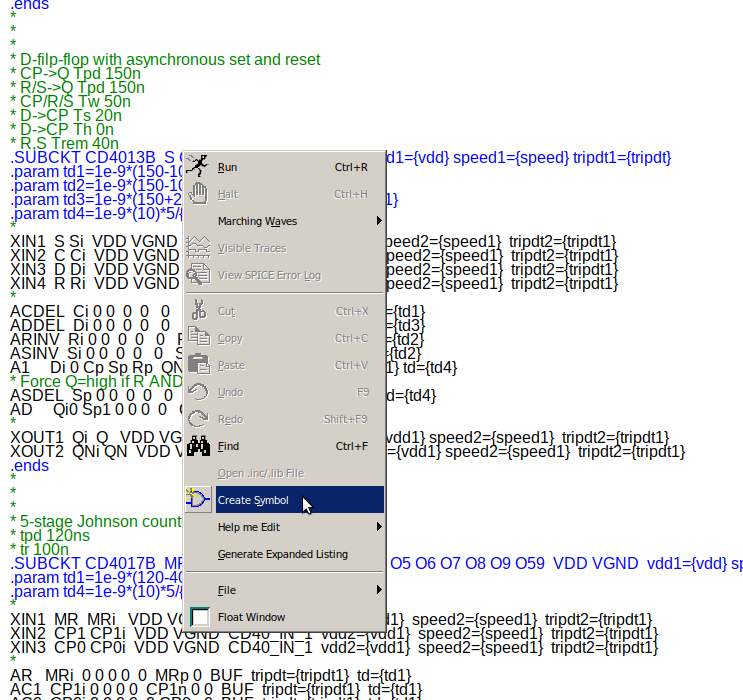
Scroll through the .lib file and find the definition (“.SUBCKT”) of the gate that you want to use. In our example we want to create a 4013 D-FlipFlop. Right-click on this line and select “Create Symbol” from the context menu
Edit the autogenerated symbol in the following way (CTRL+A opens the “Symbol Attribute Editor”):
edit the “SpiceModel” line, and enter “VDD 0”
change the “SpiceLine” line to “VDD=5 SPEED=1.0 TRIPDT=1e-9”
delete the absolute path in “ModelFile”, it should only read “CD4000_v.lib”
lastly change “Symbol Type” from “Block” to “Cell”
close the Attribute Editor and delete the GND and the VDD pin (sounds weird, but do it!). The delete button does not work in the symbol editor, do right-click and then select “delete” from the context menu.
Now click on File/Save As and save a copy of this symbol in your project directory (e.g. “/path/to/project/CD4013B.asy”)
Now go to your main SPICE simulation file and add a component. Don’t take a symbol from the symbol lib, but choose your project directory from the “Top Directory” dropdown menu. Now select the symbol you just created and insert it into your simulation sheet.
Create a voltage source with the desired operating voltage (e.g. 5V or 3.3V) and put a net label with the name “VDD” on that voltage. This will be the VDD of all your 4000-series ICs. Likewise, all 4000 ICs are automatically connected to GND.
You should probably also change VDD to 3.3 in the SPICE attribute line underneath the IC symbol if you use 3.3V. However, it does not seem to make a big difference.
You are ready to go. Simulate your circuit. If the ICs are reacting too slowly, you can change the SPEED parameter from 1.0 to 0.1, then they operate in the nanosecond regime. Yes – smaller “SPEED” parameter means faster *speed*, confusing, I know. The TRIPDT parameter, however, does not influence the steepness of your edges (but the propagation delay through the gates … or something).
You can download the example project (LTSpice sheet and symbols) HERE.
Introduction Heya. So I found people building perpetual self-exciting pendulums (pendula? pendulae?) and showing them off on youtube. Nice 🙂 So far the most elegant that I know of seems […]
Show full content
Introduction
Heya. So I found people building perpetual self-exciting pendulums (pendula? pendulae?) and showing them off on youtube. Nice So far the most elegant that I know of seems to be THIS ONE by youtube channel [TinselKoala] … which is in turn a “cover version” of some original circuit by David Williams, published in the magazine(?) “Nuts & Volts” in August 2012. The circuit is shown at the very end of TK’s video.
The basic idea is: You have a magnet on a string – the pendulum – which swings by a coil that acts both as a sensor (detecting the magnet is above) and an electromagnetic motor (giving the magnet a repulsive kick). Obviously the kicking has to occur at exactly the right time, i.e. when the magnet just barely swooshed past the center of the coil.
Let’s be honest: The Williams/TinselKoala circuit is very close to perfection: Only two transistors and barely a handful of passive components. Hats off! There is just two problems (arising from my ignorance):
BC556B and BC337-25 … errm I have never heard of these transistor types, I can probably buy them easily, but the thing is: I don’t have them at home.
I did not understand the circuit after staring at it for three minutes.
But I wanted to build such a pendulum the same evening. And in the end I did (as you see below). I decided to rely on an Arduino to control the behaviour. You might argue that an Arduino is overkill here, since we already know it can be done with two transistors only. But since a chinese Arduino leonardo clone (pro micro) costs me only 4€ and in return I get fine-tuning of the trigger threshold and FET switching timing and all that in software, I’d say that it’s a fair deal.
Schematic
So what’s going on here? We can view it as two separate circuits that have one component in common – The coil!
driver circuit:
The Arduino output pin drives the gate of the MOSFET (Q1). This way we can let current flow through the coil and turn it into an electromagnet. The current is provided by the 470uF capacitor (C1) which previously has been charged to 5V through the 100R resistor (R1). C1 is recharged, once the MOSFET is turned off again. Although very briefly there are up to 2A flowing through the coil, the power source never sees this dramatic current spike. A diode (D1) is wired in parallel to the coil and shorts it, when the FET opens and the voltage across the coil shoots up because of self-induction. Blah blah, just coil magic – just think of it like this: The energy of the magnetic field wants to go somewhere. And we tell the coil: Please dump your excess energy into the diode, rather than destroy the FET. Thank you very much.
sensor circuit:
When the FET is turned off and C1 is fully charged again, then one end of the coil is at 5V and the other end is not really connected to anything. When the coil is sensing changes in external magnetic fields, the voltage at the FET side (open end) of the coil will wiggle around and display the signal that the coil picked up. We use 1uF as an AC-coupling capacitor to connect this end of the coil to a simple inverting amplifier. In the following video I have disabled the drive pulse and we can see what comes out of the sensor circuit, i.e. what the Arduino ADC sees:
What the Arduino ADC pin sees
Code
In the above video you see that the signal that comes out of the sensor amplifier is a wiggle that first rises above the baseline, then way below the baseline, then above the baseline again and then returns to the baseline:
(picture manually redrawn for beauty)
What the Arduino shall do is:
Measure the baseline once when the device is turned on. Whenever we read the ADC value we want the baseline subtracted from it. This is done by the functions adjust_baseline() and sense().
Detect a pulse. There are several ways. I went for the following: Wait for the signal to rise above a cercain threshold, then wait until it sinks below the baseline. Now we can be pretty sure that the magnet is above the coil.
Turn the FET on for a certain time (in my case 20 ms)
Turn the FET off and don’t do anything for a while (100 ms). We don’t want the Arduino read its ADC during the switching and the recharging. Let’s just ignore all sensor data during the period where the coil is not a sensor but a driver.
GOTO 2.
Here is the Arduino code (works on ANY Arduino or Arduino compatible board):
const int FET_PIN = 10;  // digital pin 10
const int SENSE_PIN = 2; // A2 pin

const int threshold = 35; // sensor threshold above baseline

// all delays are defined in ms
const int pulse_off_delay = 100;
const int pulse_on_delay = 20;
const int pulse_pre_delay = 0;

int baseline = 0;

void adjust_baseline(){
  int accumulator = 0;
  int n = 10;
  for (int i = 0; i < n; i++){
    delay(10);
    accumulator += analogRead(SENSE_PIN);
  }
  baseline = accumulator/n;
}

void pulse(void){
  delay(pulse_pre_delay);
  digitalWrite(FET_PIN,HIGH);
  delay(pulse_on_delay);
  digitalWrite(FET_PIN,LOW);
  delay(pulse_off_delay);
}

int sense(void){
  return analogRead(SENSE_PIN)-baseline;
}

void setup() {
  // init output pin
  digitalWrite(FET_PIN,LOW);
  pinMode(FET_PIN, OUTPUT);
  delay(200);
  adjust_baseline();
}

void loop() {

  // wait for sensor > threshold
  // -> magnet approaches coil
  while(not(sense() > threshold)){
    // do nothing
  }

  // wait until sensor < 0
  // -> magnet just above coil center
  while(not(sense() < 0)){
    // do nothing
  }

  // switch FET, make pulse
  // -> repulse magnet
  pulse();

}
The Coil
One more word about the coil. I used 0.15mm diameter lacquer coated copper wire wound around the above 3d-printed spool. I didn’t count the windings, but l sorta filled up the spool up to the beginning of the outer tiny holes. Here is the spool’s STL file. And here is the SCAD script that created the shape. You see the hexagonal hole in the middle? That shape is not random … this way you can put the spool on the shaft of an electric screwdriver to wind the coil. In the end my coil had a DC resistance of slightly more than 3 Ohms. The pendulum only works with the right orientation of the coil towards a particular pole of the magnet. If you observe that the coil is decelerating the pendulum instead of exciting it, then flip either the magnet or the coil.
Conclusion
That’s it. Build your own pendulum. Be happy. If you succeed send me pictures or videos.


 Enjoy.